

 This topic is locked
Many people confuse the terms memory and storage, particularly when describing the amount they have of each. Memory refers to the amount of RAM installed in a computer, while the term storage refers to the capacity of the computer's hard disk drive. To clarify this common mix-up, let's compare your computer to an office that contains a filing cabinet, a desk, and you.
The filing cabinet represents the computer's hard drive, which provides storage for all the files and information you need in your office. When you come in to work, you take out the files you need from the filing cabinet and put them on your desk for easy access while you work on them. The desk is like the memory in a computer, that is, it holds the information you need to have handy while you are working. You will be the processor in this example.
Consider the filing cabinet and desk analogy for a moment. Think about what it would be like if every time you wanted to look at a document, you had to get up and get it from the filing cabinet. This extra step would not only slow things down tremendously, it will also put added stress on you (processor). With adequate desk space (memory) you can lay out the documents you're using and find the information in them quickly and easily, allowing you to work more efficiently and with less stress.
Another important difference between memory and storage is that the information stored on a hard drive remains intact...even when the computer is powered down, but any data in the memory is lost when the computer is turned off. In our desk space analogy, it's like the cleaning crew throwing out anything left on the desk at the end of the day.
Types of Memory
To understand the different types of memory, you'll need a basic understanding of how it stores and accesses information.
SAM or Serial Access Memory stores data as a series of memory cells that can only be accessed sequentially (like links on a chain). If the data is not in the current location, each memory cell is checked until the needed data is found. SAM works very well for memory buffers, where the data is normally stored in the order in which it will be used, like buffer memory on a video card, but is pretty inefficient in other applications. RAM data, on the other hand, can be accessed in any order at any time.
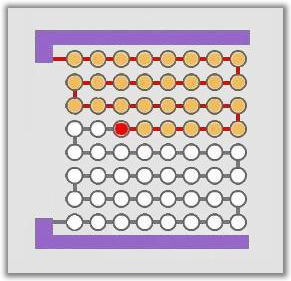
RAM or Random Access Memory is the best known type of computer memory. RAM is considered "random access" because you can access any memory cell directly if you know the row and column that intersect at that cell. This column/row location is the cell's memory address or memory location.
DRAM or Dynamic Random Access Memory. Similar to a microprocessor, a memory chip is an integrated circuit made of millions of transistors and capacitors etched in pairs on a silicon wafer. Each of these pairs forms a memory cell, in which is stored a single bit of data as a 0 or a 1. The capacitor holds the bit of information, while the transistor acts as a switch that lets the control circuitry on the memory chip read the capacitor or change its state.
Think of the capacitor as a small bucket that is able to store an electrical charge. To store a 1 in the memory cell, the bucket is filled with electricity. To store a 0, it's emptied. The problem is, the bucket has a hole in it. Over time, a full bucket becomes empty. So for dynamic memory to work, either the CPU or the memory controller has to come along and refill all of the buckets holding a 1 before they empty. To do this, the memory controller reads the memory and then writes it back. This refresh process happens thousands of times per second and is measured in nanoseconds (ns).
This refreshing process is where Dynamic RAM gets its name. Dynamic RAM has to be dynamically refreshed constantly or it forgets what it's storing. The downside of all of this refreshing is that it takes time and slows down the memory. Memory cells are etched onto silicon wafers in an array of columns (called bitlines or CAS) and rows ( called wordlines or RAS). The cell where a bitline and wordline converge constitutes the address of the memory cell...or it's memory location.
DRAM works by sending a signal through the appropriate column (CAS in the image above) to activate the transistor at each bit in the column. When writing, the row lines contain the state the capacitor should take on. When reading, the sense-amplifier determines the level of charge in the capacitor. If it's more than 50 percent, it reads it as a 1, less than 50% and it is seen as a 0. The counter tracks the refresh sequence based on which rows have been accessed and in what order. The length of time necessary to do all this is expressed in nanoseconds (billionths of a second). A memory chip rating of 70ns means that it takes 70 nanoseconds to completely read and recharge each cell.
Memory cells alone would be worthless without some way to get information in and out of them. So the memory cells have a whole infrastructure of specialized circuitry. These circuits perform such tasks as:
- Telling a cell whether to refresh or not (Write Enable)
- Keeping track of the refresh sequence (Counter)
- Identifying each row and column (RAS and CAS)
- Reading and restoring a cell's state (Sense Amplification)
Static RAM is fast and expensive, and dynamic RAM is less expensive and slower. So static RAM is used to create the CPU's speed-sensitive cache, while dynamic RAM forms the larger system RAM.
FPM DRAM or Fast Page Mode Dynamic RAM was the original form of DRAM. It waits through the entire process of locating a bit of data by column and row and reading the bit before it starts on the next bit. Maximum transfer rate to L2 cache is about 176 MBps.
EDO DRAM or Extended Data-Out Dynamic RAM does not wait for all of the processing of the first bit before continuing to the next one. As soon as the address of the first bit is located, EDO DRAM begins looking for the next bit. It is about 5% faster than FPM. Maximum transfer rate to L2 cache is about 264 MBps.
SDRAM or Synchronous Dynamic RAM takes advantage of the burst mode concept to greatly improve performance. It does this by staying on the row containing the requested bit and moving rapidly through the columns, reading each bit as it goes. The idea is that most of the time the data needed by the CPU will be in sequence. SDRAM is about 5% faster than EDO RAM and is the most common form in desktops today. Maximum transfer rate to L2 cache is about 528 MBps.
DDR SDRAM or Double Data Rate Synchronous Dynamic RAM is just like SDRAM except that is has higher bandwidth, meaning greater speed. Maximum transfer rate to L2 cache is approximately 1,064 MBps (for DDR SDRAM 133 MHZ).
RDRAM or Rambus Dynamic RAM is a radical departure from the previous DRAM architecture. Designed by Rambus, RDRAM uses a Rambus In-line Memory Module (RIMM), which is similar in size and pin configuration to a standard DIMM. What makes RDRAM so different is its use of a special high-speed data bus called the Rambus channel. RDRAM memory chips work in parallel to achieve a data rate of 800 MHz, or 1,600 MBps. Since they operate at such high speeds, they generate a lot more heat than other types of memory chips. To help dissipate the excess heat Rambus chips are fitted with a heat spreader or heat sink, which looks like a long thin wafer. Just like there are smaller versions of DIMMs, there are also SO-RIMMs, designed for notebook computers.
Memory chips in early desktop computers used a pin configuration called DIP, or Dual Inline Package. This pin configuration could be soldered into holes on the computer's mainboard or inserted into a socket soldered on the mainboard. This worked fine when computers operated on a few megabytes of memory, but as requirements for memory increased, the number of chips required on the mainboard also increased.
The solution was to place the memory chips, along with all of the support components, on a separate printed circuit board that could be inserted into a special connector or slot on the mainboard. Most of these chips use an SOJ (Small Outline J-lead) pin configuration, but quite a few manufacturers use the TSOP (Thin Small Outline Package configuration as well. The key difference between these newer pin types and the original DIP configuration is that SOJ and TSOP chips are surface-mounted to the printed circuit. In other words, the pins are soldered directly to the surface of the board, not inserted in holes or sockets.
Memory chips are normally only available as part of a card called a module. You've probably seen memory listed as 8x32 or 4x16. These numbers represent the number of the chips multiplied by the capacity of each chip, which is measured in megabits (Mb), or one million bits. Take the result and divide it by eight to get the number of megabytes on that module. For example, 4x32 means that the module has four 32-megabit chips. Multiply 4 by 32 and you get 128 megabits. Since we know that a byte has 8 bits, we need to divide the result by 8...which gives us 16 megabytes (MB).
=================================================
Memory Timings
The topic of memory architecture is too detailed and complex to cover in a single tutorial, but we'll try to simplify a portion of it to address memory timings and how they work...albeit briefly.
The performance and stability of any system depends in part on the memory being used and the settings for the RAM timing. Many users may prefer "this" brand as opposed to "that" brand, and certainly using brand name memory is a very good idea since low quality memory is often at the root of many stability issues. However, it is also important to pay attention to the timing settings of the memory used.
Typical timing parameters appear as 2-3-2-6-T1 or some variant. So what do these numbers mean?
Before delving into these specific settings, let's first define some common terms used when discussing memory timings.
- RAS - Row Address Strobe or Row Address Select
- CAS - Column Address Strobe or Column Address Select
- tRAS - Active to precharge delay; this is the delay between the precharge and activation of a row
- tRCD - RAS to CAS Delay; the time required between RAS and CAS access
- tCL - (or CL) CAS Latency
- tRP - RAS Precharge; the time required to switch from one row to the next row, for example, switch internal memory banks
- tCLK ClocK; the length of a clock cycle
- Command Rate - the delay between Chip Select (CS), or when an IC is selected and the time commands can be issued to the IC
- Latency - The time from when a request is made to when it is answered; the total time required before data can be written to or read from the memory.
tRAS
Memory architecture is like a spreadsheet with row upon row and column upon column, with each row being one bank. For the processor to access memory, it first must determine which row or bank in the memory is to be accessed and then activate that row with the RAS signal. Once activated, the row can be accessed over and over, until the data is exhausted. This is why tRAS has little effect on overall system performance but could impact system stability if set incorrectly.
tRCD
tRCD is the delay from the time a row is activated to when the cell (or column) is activated by the CAS signal and data can be written to or read from a memory cell. When memory is accessed sequentially, the row is already active and tRCD will not have much impact. However, if memory is not accessed in a linear fashion, the current active row must be deactivated and then a new row selected/activated. In such an example, low tRCD's can improve performance. However, like any other memory timing, putting this too low for the module can cause in instability.
CAS Latency
Certainly, one of the most important timings is the CAS Latency, which is also the one most people understand. Since data is often accessed sequentially (same row), the CPU need only select the next column in the row to get the next piece of data. In other words, CAS Latency is the delay between the CAS signal and the availability of valid data on the data pins (DQ). The latency between column accesses (CAS) then plays an important role in the performance of the memory. The lower the latency, the better the performance. However, the memory modules must be able to support low-latency settings.
tRP
tRP is the time required to terminate one row access and begin the next row access. tRP might also be seen as the delay required between deactivating the current row and selecting the next row. So in conjunction with tRCD, the time required (or clock cycles required) to switch banks (or rows) and select the next cell for reading, writing, or refreshing is a combination of tRP and tRCD.
tRAS
tRAS is the time required before (or delay needed) between the active and precharge commands. In other words, how long the memory must wait before the next memory access can begin.
tCLK
This is simply the clock used for the memory. Note that because frequency is 1/t, if memory were running at 100Mhz, the timing of the memory would be 1/100Mhz, or 10nS.
Command Rate
The Command Rate is the time needed between the chip select signal and when commands can be issued to the RAM module IC. Typically, these are either 1 clock or 2.
=================================================
Latency
If youre in the market for some new memory, you will see modules ranging widely in price. The cheaper memory might not be as attractive, maybe no heatsinks, while the more expensive memory can come with anything from colored heatsinks to L.E.D.s. Both are rated at the same speed, so are you paying all that extra money for the colored heatsink and flashing LED.s? Most likely not, each contains different chips, with different CAS latency. We'll explore what exactly memory latency is, and how it affects your systems performance.
What is Memory Latency?
When we see what a RAMs CAS latency is, it's 4 numbers, such as 2-2-2-5, which correspond with CAS tRCD tRP tRAS. You should be able to change the CAS Latency in your BIOS. In most BIOS versions, it can be found under the advanced chipset menu, though it can be found in different areas in different BIOS versions.
CAS stands for Column Address Strobe. This is the number of memory cycles that pass between the time a column is requested from the active page and the time the data is ready to send across the bus. This number is usually 2, 2.5, and 3, on DDR memory.
RAS to CAS Delay is referred to as tRCD. This is the delay in memory cycles between the time a row is activated and when data within the row can be requested. This only happens when data is not on the active row.
tRP is the time for RAS Precharge. This is the time in memory cycles that is required to clear the active row out of the cache, before a new row can be requested. In other words, its the time it takes for the memory to stop accessing one row and start accessing another. Once again this only takes place if the data is not in the active row.
tRAS refers to the minimum time that a row must remain active before a new row can be activated in each memory bank. A new row can not be opened until the minimum amount of time has passed. If there is more than one bank on memory, this will help the performance of the tRAS. If there is only one active bank, then the need to change rows is guaranteed, and if there is more than one bank with memory, then there is only half the chance that there will be a need to change rows. In turn, the tRAS will only come into effect half the time. The tRP and tRAS together are often referred to as the Row Cycle time, because they happen together.
Let's compare this to a library. Say you want a book about Montana and, for our example, let's say the librarian is putting books away when you ask for a book on Montana. The librarian would have to get off the ladder, move the ladder to the travel section, and then get back up on the ladder. This would compare with the tRP. The tRCD would be the time the librarian is at the right shelf and right row of the bookcase. The tRAS would be the time when the librarian finds the books about Montana, and when they find the specific book you want. The CAS latency, in this case, would be the time from when they take the book off the shelf, and the time it takes them to walk back to you. If they walk fast, it might be 2; if they walk slower, the number would be larger.
Now let's say the librarian is putting the book on Montana back. The time required would be a lot less because the ladder would not have to be moved...it's already at the correct location. This would happen in the memory if the data needed is on the active row.
================================================


 Sign In
 Create Account
