


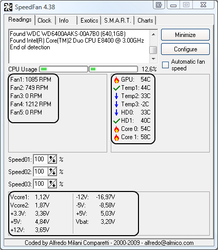
EDIT: Before I replaced the RAM and HDD, the restarts/lockups were VERY frequent in occurrence (sometimes around every 5 minutes), now its only a few times a day.
CPU-Z TXT Report
-------------------------------------------------------------------------

Binaries
-------------------------------------------------------------------------

CPU-Z version			1.53.1

Processors
-------------------------------------------------------------------------

Number of processors		1
Number of threads		2

APICs
-------------------------------------------------------------------------

Processor 0
	-- Core 0
		-- Thread 0	0
	-- Core 1
		-- Thread 0	1

Processors Information
-------------------------------------------------------------------------

Processor 1			ID = 0
	Number of cores		2 (max 2)
	Number of threads	2 (max 2)
	Name			AMD Athlon 64 X2 3800+
	Codename		Windsor
	Specification		AMD Athlon(tm) 64 X2 Dual Core Processor 3800+
	Package 		Socket AM2 (940)
	CPUID			F.B.2
	Extended CPUID		F.4B
	Brand ID		4
	Core Stepping		BH-F2
	Technology		90 nm
	Core Speed		2000.1 MHz
	Multiplier x FSB	10.0 x 200.0 MHz
	HT Link speed		1000.0 MHz
	Stock frequency		2000 MHz
	Instructions sets	MMX (+), 3DNow! (+), SSE, SSE2, SSE3, x86-64, AMD-V
	L1 Data cache		2 x 64 KBytes, 2-way set associative, 64-byte line size
	L1 Instruction cache	2 x 64 KBytes, 2-way set associative, 64-byte line size
	L2 cache		2 x 512 KBytes, 16-way set associative, 64-byte line size
	FID/VID Control		yes
	Max FID			10.0x
	Max VID			1.350 V

	K8 Thermal sensor	yes
	K8 Revision ID		5.2
	Attached device		PCI device at bus 0, device 24, function 0
	Attached device		PCI device at bus 0, device 24, function 1
	Attached device		PCI device at bus 0, device 24, function 2
	Attached device		PCI device at bus 0, device 24, function 3


Thread dumps
-------------------------------------------------------------------------

CPU Thread 0
	APIC ID			0
	Topology		Processor ID 0, Core ID 0, Thread ID 0
	Type			02002008h
	Max CPUID level		00000001h
	Max CPUID ext. level	80000018h
	Cache descriptor	Level 1, I, 64 KB, 1 thread(s)
	Cache descriptor	Level 1, D, 64 KB, 1 thread(s)
	Cache descriptor	Level 2, U, 512 KB, 1 thread(s)

	CPUID
	0x00000000		0x00000001	0x68747541	0x444D4163	0x69746E65
	0x00000001		0x00040FB2	0x00020800	0x00002001	0x178BFBFF
	0x80000000		0x80000018	0x68747541	0x444D4163	0x69746E65
	0x80000001		0x00040FB2	0x0000090D	0x0000001F	0xEBD3FBFF
	0x80000002		0x20444D41	0x6C687441	0x74286E6F	0x3620296D
	0x80000003		0x32582034	0x61754420	0x6F43206C	0x50206572
	0x80000004		0x65636F72	0x726F7373	0x30383320	0x00002B30
	0x80000005		0xFF08FF08	0xFF20FF20	0x40020140	0x40020140
	0x80000006		0x00000000	0x42004200	0x02008140	0x00000000
	0x80000007		0x00000000	0x00000000	0x00000000	0x0000003F
	0x80000008		0x00003028	0x00000000	0x00000001	0x00000000
	0x80000009		0x00000000	0x00000000	0x00000000	0x00000000
	0x8000000A		0x00000001	0x00000040	0x00000000	0x00000000
	0x8000000B		0x00000000	0x00000000	0x00000000	0x00000000
	0x8000000C		0x00000000	0x00000000	0x00000000	0x00000000
	0x8000000D		0x00000000	0x00000000	0x00000000	0x00000000
	0x8000000E		0x00000000	0x00000000	0x00000000	0x00000000
	0x8000000F		0x00000000	0x00000000	0x00000000	0x00000000
	0x80000010		0x00000000	0x00000000	0x00000000	0x00000000
	0x80000011		0x00000000	0x00000000	0x00000000	0x00000000
	0x80000012		0x00000000	0x00000000	0x00000000	0x00000000
	0x80000013		0x00000000	0x00000000	0x00000000	0x00000000
	0x80000014		0x00000000	0x00000000	0x00000000	0x00000000
	0x80000015		0x00000000	0x00000000	0x00000000	0x00000000
	0x80000016		0x00000000	0x00000000	0x00000000	0x00000000
	0x80000017		0x00000000	0x00000000	0x00000000	0x00000000
	0x80000018		0x00000000	0x00000000	0x00000000	0x00000000

	MSR 0x0000001B		0x00000000	0xFEE00900
	MSR 0xC001001E		0x00000000	0x00000052
	MSR 0xC0010015		0x00000000	0x02000040
	MSR 0xC0010042		0x3108120A	0x080C020C
	MSR 0xC0010041		0x00000001	0x00000A0C

CPU Thread 1
	APIC ID			1
	Topology		Processor ID 0, Core ID 1, Thread ID 0
	Type			02002008h
	Max CPUID level		00000001h
	Max CPUID ext. level	80000018h
	Cache descriptor	Level 1, I, 64 KB, 1 thread(s)
	Cache descriptor	Level 1, D, 64 KB, 1 thread(s)
	Cache descriptor	Level 2, U, 512 KB, 1 thread(s)

	CPUID
	0x00000000		0x00000001	0x68747541	0x444D4163	0x69746E65
	0x00000001		0x00040FB2	0x01020800	0x00002001	0x178BFBFF
	0x80000000		0x80000018	0x68747541	0x444D4163	0x69746E65
	0x80000001		0x00040FB2	0x0000090D	0x0000001F	0xEBD3FBFF
	0x80000002		0x20444D41	0x6C687441	0x74286E6F	0x3620296D
	0x80000003		0x32582034	0x61754420	0x6F43206C	0x50206572
	0x80000004		0x65636F72	0x726F7373	0x30383320	0x00002B30
	0x80000005		0xFF08FF08	0xFF20FF20	0x40020140	0x40020140
	0x80000006		0x00000000	0x42004200	0x02008140	0x00000000
	0x80000007		0x00000000	0x00000000	0x00000000	0x0000003F
	0x80000008		0x00003028	0x00000000	0x00000001	0x00000000
	0x80000009		0x00000000	0x00000000	0x00000000	0x00000000
	0x8000000A		0x00000001	0x00000040	0x00000000	0x00000000
	0x8000000B		0x00000000	0x00000000	0x00000000	0x00000000
	0x8000000C		0x00000000	0x00000000	0x00000000	0x00000000
	0x8000000D		0x00000000	0x00000000	0x00000000	0x00000000
	0x8000000E		0x00000000	0x00000000	0x00000000	0x00000000
	0x8000000F		0x00000000	0x00000000	0x00000000	0x00000000
	0x80000010		0x00000000	0x00000000	0x00000000	0x00000000
	0x80000011		0x00000000	0x00000000	0x00000000	0x00000000
	0x80000012		0x00000000	0x00000000	0x00000000	0x00000000
	0x80000013		0x00000000	0x00000000	0x00000000	0x00000000
	0x80000014		0x00000000	0x00000000	0x00000000	0x00000000
	0x80000015		0x00000000	0x00000000	0x00000000	0x00000000
	0x80000016		0x00000000	0x00000000	0x00000000	0x00000000
	0x80000017		0x00000000	0x00000000	0x00000000	0x00000000
	0x80000018		0x00000000	0x00000000	0x00000000	0x00000000

	MSR 0x0000001B		0x00000000	0xFEE00800
	MSR 0xC001001E		0x00000000	0x00000052
	MSR 0xC0010015		0x00000000	0x02000040
	MSR 0xC0010042		0x3108120A	0x080C020C
	MSR 0xC0010041		0x00000001	0x00000A0C


Chipset
-------------------------------------------------------------------------

Northbridge			NVIDIA nForce 570 Ultra rev. A1
Southbridge			NVIDIA nForce 570 Ultra rev. A2
Graphic Interface		PCI-Express
PCI-E Link Width		x16
PCI-E Max Link Width		x16
Memory Type			DDR2
Memory Size			4096 MBytes
Channels			Dual
Memory Frequency		400.0 MHz (CPU/5)
CAS# latency (CL)		5.0
RAS# to CAS# delay (tRCD)	6
RAS# Precharge (tRP)		5
Cycle Time (tRAS)		18
Bank Cycle Time (tRC)		24
Command Rate (CR)		2T

Memory SPD
-------------------------------------------------------------------------

DIMM #				1
	SMBus address		0x51
	Memory type		DDR2
	Module format		Regular UDIMM
	Manufacturer (ID)	Wintec Industries (7F61000000000000)
	Size			2048 MBytes
	Max bandwidth		PC2-6400 (400 MHz)
	Part number
	Number of banks		2
	Data width		64 bits
	Correction		None
	Nominal Voltage		1.80 Volts
	EPP			no
	XMP			no
JEDEC timings table		CL-tRCD-tRP-tRAS-tRC @ frequency
	JEDEC #1		3.0-3-3-9-12 @ 200 MHz
	JEDEC #2		4.0-4-4-12-16 @ 266 MHz
	JEDEC #3		5.0-5-5-18-23 @ 400 MHz

DIMM #				2
	SMBus address		0x53
	Memory type		DDR2
	Module format		Regular UDIMM
	Manufacturer (ID)	Wintec Industries (7F61000000000000)
	Size			2048 MBytes
	Max bandwidth		PC2-6400 (400 MHz)
	Part number
	Number of banks		2
	Data width		64 bits
	Correction		None
	Nominal Voltage		1.80 Volts
	EPP			no
	XMP			no
JEDEC timings table		CL-tRCD-tRP-tRAS-tRC @ frequency
	JEDEC #1		3.0-3-3-9-12 @ 200 MHz
	JEDEC #2		4.0-4-4-12-16 @ 266 MHz
	JEDEC #3		5.0-5-5-18-23 @ 400 MHz

DIMM #				1
SPD registers
		00 01 02 03 04 05 06 07 08 09 0A 0B 0C 0D 0E 0F
	00	80 08 08 0E 0A 61 40 00 05 25 40 00 82 08 00 00
	10	0C 08 38 01 02 00 03 3D 50 50 60 32 1E 32 2D 01
	20	17 25 05 12 3C 1E 1E 00 36 39 7F 80 14 1E 00 00
	30	00 00 00 00 00 00 00 00 00 00 00 00 00 00 12 F9
	40	7F 61 00 00 00 00 00 00 00 00 00 00 00 00 00 00
	50	00 00 00 00 00 00 00 00 00 00 00 00 00 00 00 00
	60	00 00 00 00 00 00 00 00 00 00 00 00 00 00 00 00
	70	00 00 00 00 00 00 00 00 00 00 00 00 00 00 00 00
	80	FF FF FF FF FF FF FF FF FF FF FF FF FF FF FF FF
	90	FF FF FF FF FF FF FF FF FF FF FF FF FF FF FF FF
	A0	FF FF FF FF FF FF FF FF FF FF FF FF FF FF FF FF
	B0	FF FF FF FF FF FF FF FF FF FF FF FF FF FF FF FF
	C0	FF FF FF FF FF FF FF FF FF FF FF FF FF FF FF FF
	D0	FF FF FF FF FF FF FF FF FF FF FF FF FF FF FF FF
	E0	FF FF FF FF FF FF FF FF FF FF FF FF FF FF FF FF
	F0	FF FF FF FF FF FF FF FF FF FF FF FF FF FF FF FF

DIMM #				2
SPD registers
		00 01 02 03 04 05 06 07 08 09 0A 0B 0C 0D 0E 0F
	00	80 08 08 0E 0A 61 40 00 05 25 40 00 82 08 00 00
	10	0C 08 38 01 02 00 03 3D 50 50 60 32 1E 32 2D 01
	20	17 25 05 12 3C 1E 1E 00 36 39 7F 80 14 1E 00 00
	30	00 00 00 00 00 00 00 00 00 00 00 00 00 00 12 F9
	40	7F 61 00 00 00 00 00 00 00 00 00 00 00 00 00 00
	50	00 00 00 00 00 00 00 00 00 00 00 00 00 00 00 00
	60	00 00 00 00 00 00 00 00 00 00 00 00 00 00 00 00
	70	00 00 00 00 00 00 00 00 00 00 00 00 00 00 00 00
	80	FF FF FF FF FF FF FF FF FF FF FF FF FF FF FF FF
	90	FF FF FF FF FF FF FF FF FF FF FF FF FF FF FF FF
	A0	FF FF FF FF FF FF FF FF FF FF FF FF FF FF FF FF
	B0	FF FF FF FF FF FF FF FF FF FF FF FF FF FF FF FF
	C0	FF FF FF FF FF FF FF FF FF FF FF FF FF FF FF FF
	D0	FF FF FF FF FF FF FF FF FF FF FF FF FF FF FF FF
	E0	FF FF FF FF FF FF FF FF FF FF FF FF FF FF FF FF
	F0	FF FF FF FF FF FF FF FF FF FF FF FF FF FF FF FF


Monitoring
-------------------------------------------------------------------------

Mainboard Model		MS-7250 (0x0000019B - 0x005F1AD0)

LPCIO
-------------------------------------------------------------------------

LPCIO Vendor		Winbond
LPCIO Model		W83627EHF
LPCIO Vendor ID		0x5CA3
LPCIO Chip ID		0x88
LPCIO Revision ID	0x68
Config Mode I/O address	0x4E
Config Mode LDN		0xB
Config Mode registers
		00 01 02 03 04 05 06 07 08 09 0A 0B 0C 0D 0E 0F
	00	FF FF FF FF FF FF FF 0B FF FF FF FF FF FF FF FF
	10	FF FF FF FF FF FF FF FF FF FF FF FF FF FF FF FF
	20	88 68 FF 00 04 00 40 FF 50 01 00 00 02 21 00 FF
	30	01 FF FF FF FF FF FF FF FF FF FF FF FF FF FF FF
	40	FF FF FF FF FF FF FF FF FF FF FF FF FF FF FF FF
	50	FF FF FF FF FF FF FF FF FF FF FF FF FF FF FF FF
	60	0A 10 FF FF FF FF FF FF FF FF FF FF FF FF FF FF
	70	00 FF FF FF FF FF FF FF FF FF FF FF FF FF FF FF
Register space		LPC, base address = 0x0A10


Hardware Monitors
-------------------------------------------------------------------------

Hardware monitor	Winbond W83627EHF
	Voltage 0	1.27 Volts [0x9F] (CPU VCORE)
	Voltage 1	1.82 Volts [0xE4] (VIN0)
	Voltage 2	3.28 Volts [0xCD] (AVCC)
	Voltage 3	3.28 Volts [0xCD] (+3.3V)
	Voltage 4	1.60 Volts [0xC8] (VIN1)
	Voltage 5	1.41 Volts [0xB0] (VIN2)
	Voltage 6	1.42 Volts [0xB1] (VIN3)
	Voltage 7	1.48 Volts [0xB9] (VIN4)
	Temperature 0	38°C (100°F) [0x26] (SYSTIN)
	Temperature 1	44°C (111°F) [0x1A8] (CPUTIN)
	Temperature 2	45°C (113°F) [0x1A6] (AUXTIN)
	Fan 0		2557 RPM [0x42] (SYSFANIN)
	Fan 3		3309 RPM [0x33] (CPUFANIN1)
Hardware registers
Register space		LPC, base address = 0x0A10
bank 0
		00 01 02 03 04 05 06 07 08 09 0A 0B 0C 0D 0E 0F
	00	04 FF 04 FF 01 00 00 00 01 01 01 01 3C 3C 01 01
	10	04 FF 40 00 00 01 01 3C 43 07 00 00 57 00 00 C3
	20	A0 E6 CD CD CA AF B0 26 42 FF FF DA 00 FF FF FF
	30	BB F9 E7 FE DF FE F7 FF FF C7 FF FF D6 FF DF 33
	40	03 9A 17 DE FF FF 00 F4 2D FF 40 C4 10 95 00 A3
	50	FF FF 80 FF FF FF 00 80 A1 7F FF FF 19 01 FF 05
	60	04 FF 40 00 01 01 3C FF 01 FF 01 FF FF FF FF FF
	70	FF FF FF FF FF FF FF FF FF FF FF FF FF FF FF FF
	80	04 FF 04 FF 01 00 00 00 01 01 01 01 3C 3C 01 01
	90	04 FF 40 00 00 01 01 3C 43 07 00 00 57 00 00 C5
	A0	A0 E5 CD CD CA AF B0 26 42 FF FF DA 00 FF FF FF
	B0	BB F9 E7 FE DF FE F7 FF FF C7 FF FF D6 FF DF 33
	C0	03 00 10 DE FF FF 00 F4 2D FF 40 C4 10 95 00 A3
	D0	FF FF 80 FF FF FF 00 80 A1 7F FF FF 19 01 FF 05
	E0	04 FF 40 00 01 01 3C FF 01 FF 01 FF FF FF FF FF
	F0	FF FF FF FF FF FF FF FF FF FF FF FF FF FF FF FF
bank 1
	50	D4 00 00 4B 00 50 00 FF FF FF FF FF FF FF FF FF
bank 2
	50	D3 00 00 4B 00 50 00 FF FF FF FF FF FF FF FF FF
bank 3
	50	02 03 00 00 03 00 01 00 00 03 FF FF FF FF FF FF
bank 4
	50	12 13 FF 00 00 00 00 FF 74 9A 11 32 C9 FF FF FF
bank 5
	50	CB B7 B9 FF FF 9E 9B FF FB 1F E7 FE FF 00 00 00

Hardware monitor	AMD Athlon 64 X2 3800+
	Temperature 0	32°C (89°F) [0x51] (Core #0)
	Temperature 1	37°C (98°F) [0x56] (Core #1)

Hardware monitor	NVIDIA GeForce 9500 GT (Microsoft Corporation - WDDM v1.1)
	Temperature 0	44°C (111°F) (GPU Core)


PCI Devices
-------------------------------------------------------------------------

Description			RAM Memory Controller
Location			bus 0 (0x00), device 0 (0x00), function 0 (0x00)
Common header
	Vendor ID		0x10DE
	Model ID		0x0369
	Revision ID		0xA1
	PI			0x00
	SubClass		0x00
	BaseClass		0x05
	Cache Line		0x00
	Latency			0x00
	Header			0x00
PCI header
	Subvendor ID		0x1462
	Subsystem ID		0x7250
	Int. Line		0xFF
	Int. Pin		0x00
PCI capability
	Caps class		HyperTransport
	Caps offset		0x44
	Caps revision		1.03
	Interface type		Slave/Primary
	Link 0 width (in/out)	16 bits/16 bits
	Link 0 frequency	1000 MHz
	Link 1 width (in/out)	8 bits/8 bits
	Link 1 frequency	200 MHz
PCI capability
	Caps class		HyperTransport
	Caps offset		0xDC
	Interface type		MSI Mapping
PCI registers
		00 01 02 03 04 05 06 07 08 09 0A 0B 0C 0D 0E 0F
	00	DE 10 69 03 06 01 B0 00 A1 00 00 05 00 00 00 00
	10	00 00 00 00 00 00 00 00 00 00 00 00 00 00 00 00
	20	00 00 00 00 00 00 00 00 00 00 00 00 62 14 50 72
	30	00 00 00 00 44 00 00 00 00 00 00 00 FF 00 00 00
	40	62 14 50 72 08 DC E0 01 22 20 11 11 D0 00 00 00
	50	23 06 7F 00 03 00 00 00 00 00 03 00 00 00 00 00
	60	00 00 00 00 00 00 00 00 00 00 00 00 06 36 0A 00
	70	44 44 44 00 D0 09 00 00 11 00 00 00 11 11 88 00
	80	23 99 88 00 FA 00 64 0E 02 00 00 00 7F 00 00 00
	90	70 00 00 80 00 00 00 00 00 00 00 00 00 00 00 00
	A0	00 00 00 00 00 00 00 00 00 00 00 00 00 00 00 00
	B0	00 00 00 00 01 01 01 01 00 00 00 00 00 00 00 00
	C0	00 00 00 00 00 00 00 00 00 00 00 00 80 00 0F 0F
	D0	00 00 00 00 00 00 00 00 00 00 00 00 08 00 01 A8
	E0	00 00 E0 FE 00 00 00 00 00 00 80 00 F0 FF D0 00
	F0	00 00 00 00 00 00 00 00 00 00 00 00 00 00 00 00

Description			PCI to ISA Bridge
Location			bus 0 (0x00), device 1 (0x01), function 0 (0x00)
Common header
	Vendor ID		0x10DE
	Model ID		0x0362
	Revision ID		0xA2
	PI			0x00
	SubClass		0x01
	BaseClass		0x06
	Cache Line		0x00
	Latency			0x00
	Header			0x80
PCI header
	Address 0 (port)	0x00002F00
	Subvendor ID		0x1462
	Subsystem ID		0x7250
	Int. Line		0xFF
	Int. Pin		0x00
PCI registers
		00 01 02 03 04 05 06 07 08 09 0A 0B 0C 0D 0E 0F
	00	DE 10 62 03 0F 00 A0 00 A2 00 01 06 00 00 80 00
	10	01 2F 00 00 00 00 00 00 00 00 00 00 00 00 00 00
	20	00 00 00 00 00 00 00 00 00 00 00 00 62 14 50 72
	30	00 00 00 00 00 00 00 00 00 00 00 00 FF 00 00 00
	40	62 14 50 72 00 00 D0 FE FA 3E FF 00 FA 3E FF 00
	50	FA 3E FF 00 00 5A 62 02 00 00 00 01 00 00 FE BF
	60	00 00 00 00 00 00 00 00 00 00 00 00 00 00 F9 FF
	70	10 00 FF FF C5 80 00 00 00 00 45 19 00 00 40 00
	80	09 20 00 D2 81 D8 00 10 F0 00 00 01 F0 00 00 00
	90	00 08 00 00 00 00 00 00 21 47 95 86 EF CD AB 00
	A0	01 00 10 80 00 00 00 00 00 00 00 00 00 00 00 00
	B0	00 00 00 00 00 0A 7F 0A 00 00 00 00 00 00 00 00
	C0	00 00 00 00 00 00 00 00 00 00 00 00 00 00 00 00
	D0	00 00 00 00 00 00 00 00 44 00 00 FE FD 03 00 A0
	E0	00 00 00 00 00 00 00 00 00 00 00 00 00 00 00 00
	F0	00 00 00 00 00 00 00 00 10 00 00 00 00 00 00 00

Description			SMBus Controller
Location			bus 0 (0x00), device 1 (0x01), function 1 (0x01)
Common header
	Vendor ID		0x10DE
	Model ID		0x0368
	Revision ID		0xA2
	PI			0x00
	SubClass		0x05
	BaseClass		0x0C
	Cache Line		0x00
	Latency			0x00
	Header			0x80
PCI header
	Address 0 (port)	0x00002900
	Address 4 (port)	0x00002D00
	Address 5 (port)	0x00002E00
	Subvendor ID		0x1462
	Subsystem ID		0x7250
	Int. Line		0x0B
	Int. Pin		0x01
PCI capability
	Caps class		Power Management
	Caps offset		0x44
	Caps version		1.1
PCI registers
		00 01 02 03 04 05 06 07 08 09 0A 0B 0C 0D 0E 0F
	00	DE 10 68 03 01 00 B0 00 A2 00 05 0C 00 00 80 00
	10	01 29 00 00 00 00 00 00 00 00 00 00 00 00 00 00
	20	01 2D 00 00 01 2E 00 00 00 00 00 00 62 14 50 72
	30	00 00 00 00 44 00 00 00 00 00 00 00 0B 01 00 00
	40	62 14 50 72 01 00 02 C0 00 00 00 00 00 00 00 00
	50	00 00 00 00 00 00 00 00 00 00 00 00 00 00 00 00
	60	01 20 00 00 01 24 00 00 01 28 00 00 00 00 00 00
	70	01 00 00 00 00 00 F8 F9 00 00 00 00 01 00 00 00
	80	00 00 00 00 00 00 00 00 00 00 00 00 00 00 00 00
	90	00 00 00 00 00 00 00 00 00 00 00 00 00 00 00 00
	A0	00 00 00 00 00 00 00 00 00 00 00 00 00 00 00 00
	B0	00 00 00 00 00 00 00 00 00 00 00 00 00 00 00 00
	C0	D4 30 80 00 01 00 00 00 00 00 00 00 00 00 00 00
	D0	00 00 00 00 00 00 00 00 00 00 00 00 00 00 00 00
	E0	94 14 05 00 05 62 80 03 80 30 00 00 41 44 44 11
	F0	5A FF 5F 3F 00 00 00 C0 10 00 00 00 00 00 00 00

Description			USB Controller (OHCI)
Location			bus 0 (0x00), device 2 (0x02), function 0 (0x00)
Common header
	Vendor ID		0x10DE
	Model ID		0x036C
	Revision ID		0xA1
	PI			0x10
	SubClass		0x03
	BaseClass		0x0C
	Cache Line		0x00
	Latency			0x00
	Header			0x80
PCI header
	Address 0 (memory)	0xF9FFB000
	Subvendor ID		0x1462
	Subsystem ID		0x7250
	Int. Line		0x17
	Int. Pin		0x01
PCI capability
	Caps class		Power Management
	Caps offset		0x44
	Caps version		1.1
PCI registers
		00 01 02 03 04 05 06 07 08 09 0A 0B 0C 0D 0E 0F
	00	DE 10 6C 03 06 00 B0 00 A1 10 03 0C 00 00 80 00
	10	00 B0 FF F9 00 00 00 00 00 00 00 00 00 00 00 00
	20	00 00 00 00 00 00 00 00 00 00 00 00 62 14 50 72
	30	00 00 00 00 44 00 00 00 00 00 00 00 17 01 03 01
	40	62 14 50 72 01 00 02 FE 00 00 00 00 00 00 00 00
	50	10 00 00 00 1D 47 40 00 10 00 00 00 00 00 00 00
	60	00 00 00 00 00 00 00 00 00 00 00 00 00 00 00 00
	70	00 00 00 00 00 00 00 00 00 00 00 00 00 00 00 00
	80	00 00 00 00 00 00 00 00 00 00 00 00 00 00 00 00
	90	00 00 00 00 00 00 00 00 00 00 00 00 00 00 00 00
	A0	00 00 00 00 00 00 00 00 00 00 00 00 00 00 00 00
	B0	00 00 00 00 00 00 00 00 00 00 00 00 00 00 00 00
	C0	00 00 00 00 00 00 00 00 00 00 00 00 00 00 00 00
	D0	00 00 00 00 00 00 00 00 00 00 00 00 00 00 00 00
	E0	00 00 00 00 00 00 00 00 00 00 00 00 00 00 00 00
	F0	00 00 00 00 00 00 00 00 10 00 00 00 00 00 00 00

Description			USB 2.0 Controller (EHCI)
Location			bus 0 (0x00), device 2 (0x02), function 1 (0x01)
Common header
	Vendor ID		0x10DE
	Model ID		0x036D
	Revision ID		0xA2
	PI			0x20
	SubClass		0x03
	BaseClass		0x0C
	Cache Line		0x00
	Latency			0x00
	Header			0x80
PCI header
	Address 0 (memory)	0xF9FFAC00
	Subvendor ID		0x1462
	Subsystem ID		0x7250
	Int. Line		0x16
	Int. Pin		0x02
PCI capability
	Caps class		Debug Port
	Caps offset		0x44
PCI capability
	Caps class		Power Management
	Caps offset		0x80
	Caps version		1.1
PCI registers
		00 01 02 03 04 05 06 07 08 09 0A 0B 0C 0D 0E 0F
	00	DE 10 6D 03 06 00 B0 00 A2 20 03 0C 00 00 80 00
	10	00 AC FF F9 00 00 00 00 00 00 00 00 00 00 00 00
	20	00 00 00 00 00 00 00 00 00 00 00 00 62 14 50 72
	30	00 00 00 00 44 00 00 00 00 00 00 00 16 02 03 01
	40	62 14 50 72 0A 80 98 20 00 00 00 00 00 00 00 00
	50	00 00 00 00 00 00 00 00 00 00 00 00 00 00 00 00
	60	20 20 01 00 00 60 18 85 03 3C 3F 01 00 00 00 00
	70	00 00 08 05 00 10 20 80 89 3D B6 22 77 25 04 00
	80	01 00 02 FE 00 80 00 00 00 00 00 00 15 16 00 00
	90	00 01 00 00 00 00 00 00 00 00 00 00 00 00 00 00
	A0	01 00 00 00 00 00 00 C0 00 00 00 00 00 00 00 00
	B0	33 00 11 22 44 00 00 00 FF 03 00 00 00 00 00 00
	C0	10 10 2D 0D 00 00 00 00 00 00 00 00 00 00 00 00
	D0	00 00 00 00 00 00 00 00 00 00 00 00 00 00 00 00
	E0	00 00 00 00 00 00 00 00 00 00 00 00 00 00 00 00
	F0	00 00 00 00 00 00 00 00 10 00 00 00 00 00 00 00

Description			IDE Controller
Location			bus 0 (0x00), device 4 (0x04), function 0 (0x00)
Common header
	Vendor ID		0x10DE
	Model ID		0x036E
	Revision ID		0xA1
	PI			0x8A
	SubClass		0x01
	BaseClass		0x01
	Cache Line		0x00
	Latency			0x00
	Header			0x00
PCI header
	Address 4 (port)	0x0000FFA0
	Subvendor ID		0x1462
	Subsystem ID		0x7250
	Int. Line		0x00
	Int. Pin		0x00
PCI capability
	Caps class		Power Management
	Caps offset		0x44
	Caps version		1.1
PCI registers
		00 01 02 03 04 05 06 07 08 09 0A 0B 0C 0D 0E 0F
	00	DE 10 6E 03 05 00 B0 00 A1 8A 01 01 00 00 00 00
	10	00 00 00 00 00 00 00 00 00 00 00 00 00 00 00 00
	20	A1 FF 00 00 00 00 00 00 00 00 00 00 62 14 50 72
	30	00 00 00 00 44 00 00 00 00 00 00 00 00 00 03 01
	40	62 14 50 72 01 00 02 00 00 00 00 00 00 00 00 00
	50	02 F0 00 00 00 00 00 00 A8 A8 20 20 5F 00 20 20
	60	00 00 C5 C6 00 00 00 00 00 00 00 00 00 00 00 00
	70	00 00 00 00 00 00 00 00 00 00 00 00 00 00 00 00
	80	00 00 00 00 00 28 31 BF 00 00 02 38 00 00 00 00
	90	00 00 00 00 00 00 00 00 00 00 00 00 00 00 01 01
	A0	00 00 00 00 00 00 00 00 00 00 00 00 00 00 00 00
	B0	00 00 00 00 00 00 00 00 00 00 00 00 00 00 00 00
	C0	00 00 00 00 00 00 00 00 00 00 00 00 00 00 00 00
	D0	00 00 00 00 00 00 00 00 00 00 00 00 00 00 00 00
	E0	00 00 00 00 00 00 00 00 00 00 00 00 00 00 00 00
	F0	00 00 00 00 00 00 00 00 10 00 00 00 00 00 00 00

Description			IDE Controller
Location			bus 0 (0x00), device 5 (0x05), function 0 (0x00)
Common header
	Vendor ID		0x10DE
	Model ID		0x037F
	Revision ID		0xA2
	PI			0x85
	SubClass		0x01
	BaseClass		0x01
	Cache Line		0x00
	Latency			0x00
	Header			0x80
PCI header
	Address 0 (port)	0x0000D480
	Address 1 (port)	0x0000D400
	Address 2 (port)	0x0000D080
	Address 3 (port)	0x0000D000
	Address 4 (port)	0x0000CC00
	Address 5 (memory)	0xF9FF9000
	Subvendor ID		0x1462
	Subsystem ID		0x7250
	Int. Line		0x15
	Int. Pin		0x01
PCI capability
	Caps class		Power Management
	Caps offset		0x44
	Caps version		1.1
PCI registers
		00 01 02 03 04 05 06 07 08 09 0A 0B 0C 0D 0E 0F
	00	DE 10 7F 03 07 00 B0 00 A2 85 01 01 00 00 80 00
	10	81 D4 00 00 01 D4 00 00 81 D0 00 00 01 D0 00 00
	20	01 CC 00 00 00 90 FF F9 00 00 00 00 62 14 50 72
	30	00 00 00 00 44 00 00 00 00 00 00 00 15 01 03 01
	40	62 14 50 72 01 00 02 00 00 00 00 00 00 00 00 00
	50	FF 68 08 80 00 00 00 00 00 00 00 00 00 00 00 00
	60	00 00 00 00 41 0C 00 00 00 0F 06 42 00 00 00 00
	70	2C 78 C4 40 01 10 00 00 01 10 00 00 20 00 20 00
	80	00 00 00 40 00 30 F1 07 00 00 AC B8 FF F7 4D FF
	90	00 00 FF 39 00 00 00 00 06 00 06 10 7F 03 01 01
	A0	12 0A 00 18 00 00 00 00 00 00 00 00 33 31 00 02
	B0	05 CC 84 00 00 00 00 00 00 00 00 00 00 00 00 00
	C0	00 00 00 00 00 00 00 00 0A 00 0A 00 08 00 03 A8
	D0	0A 00 02 0C 42 00 00 00 00 00 00 00 0E 00 20 E0
	E0	0A 00 02 06 42 00 00 00 00 00 00 00 C0 02 D1 01
	F0	00 00 00 00 00 00 00 00 10 00 0C 00 00 00 00 00

Description			IDE Controller
Location			bus 0 (0x00), device 5 (0x05), function 1 (0x01)
Common header
	Vendor ID		0x10DE
	Model ID		0x037F
	Revision ID		0xA2
	PI			0x85
	SubClass		0x01
	BaseClass		0x01
	Cache Line		0x00
	Latency			0x00
	Header			0x80
PCI header
	Address 0 (port)	0x0000C880
	Address 1 (port)	0x0000C800
	Address 2 (port)	0x0000C480
	Address 3 (port)	0x0000C400
	Address 4 (port)	0x0000C080
	Address 5 (memory)	0xF9FF8000
	Subvendor ID		0x1462
	Subsystem ID		0x7250
	Int. Line		0x16
	Int. Pin		0x02
PCI capability
	Caps class		Power Management
	Caps offset		0x44
	Caps version		1.1
PCI registers
		00 01 02 03 04 05 06 07 08 09 0A 0B 0C 0D 0E 0F
	00	DE 10 7F 03 07 00 B0 00 A2 85 01 01 00 00 80 00
	10	81 C8 00 00 01 C8 00 00 81 C4 00 00 01 C4 00 00
	20	81 C0 00 00 00 80 FF F9 00 00 00 00 62 14 50 72
	30	00 00 00 00 44 00 00 00 00 00 00 00 16 02 03 01
	40	62 14 50 72 01 00 02 00 00 00 00 00 00 00 00 00
	50	FF 68 08 80 00 00 00 00 00 00 00 00 00 00 00 00
	60	00 00 00 00 41 0C 00 00 00 0F 06 42 00 00 00 00
	70	2C 78 C4 40 01 10 00 00 01 10 00 00 20 00 20 00
	80	00 00 00 00 EF FF FF FF 00 00 41 22 BF FF FF FF
	90	00 00 B4 3E 00 00 00 00 06 00 06 10 7F 03 01 01
	A0	12 0A 00 00 00 00 00 00 00 00 00 00 33 31 00 02
	B0	05 CC 84 00 00 00 00 00 00 00 00 00 00 00 00 00
	C0	00 00 00 00 00 00 00 00 0A 00 0A 00 08 00 03 A8
	D0	0A 00 02 06 42 00 00 00 00 00 00 00 00 00 F0 07
	E0	0A 00 02 06 42 00 00 00 00 00 00 00 00 02 03 00
	F0	00 00 00 00 00 00 00 00 10 00 0C 00 00 00 00 00

Description			IDE Controller
Location			bus 0 (0x00), device 5 (0x05), function 2 (0x02)
Common header
	Vendor ID		0x10DE
	Model ID		0x037F
	Revision ID		0xA2
	PI			0x85
	SubClass		0x01
	BaseClass		0x01
	Cache Line		0x00
	Latency			0x00
	Header			0x80
PCI header
	Address 0 (port)	0x0000C000
	Address 1 (port)	0x0000BC00
	Address 2 (port)	0x0000B880
	Address 3 (port)	0x0000B800
	Address 4 (port)	0x0000B480
	Address 5 (memory)	0xF9FF7000
	Subvendor ID		0x1462
	Subsystem ID		0x7250
	Int. Line		0x17
	Int. Pin		0x03
PCI capability
	Caps class		Power Management
	Caps offset		0x44
	Caps version		1.1
PCI registers
		00 01 02 03 04 05 06 07 08 09 0A 0B 0C 0D 0E 0F
	00	DE 10 7F 03 07 00 B0 00 A2 85 01 01 00 00 80 00
	10	01 C0 00 00 01 BC 00 00 81 B8 00 00 01 B8 00 00
	20	81 B4 00 00 00 70 FF F9 00 00 00 00 62 14 50 72
	30	00 00 00 00 44 00 00 00 00 00 00 00 17 03 03 01
	40	62 14 50 72 01 00 02 00 00 00 00 00 00 00 00 00
	50	FF 68 08 80 00 00 00 00 00 00 00 00 00 00 00 00
	60	00 00 00 00 41 0C 00 00 00 0F 06 42 00 00 00 00
	70	2C 78 C4 40 01 10 00 00 01 10 00 00 20 00 20 00
	80	00 00 00 00 FF FF FF FF 00 00 7F 13 7F FF FF FF
	90	00 00 AF 3E 00 00 00 00 06 00 06 10 7F 03 01 01
	A0	12 0A 00 00 00 00 00 00 00 00 00 00 33 31 00 02
	B0	05 CC 84 00 00 00 00 00 00 00 00 00 00 00 00 00
	C0	00 00 00 00 00 00 00 00 0A 00 0A 00 08 00 03 A8
	D0	0A 00 02 06 42 00 00 00 00 00 00 00 5F 5A 75 03
	E0	0A 00 02 06 42 00 00 00 00 00 00 00 DD 7F F0 07
	F0	00 00 00 00 00 00 00 00 10 00 0C 00 00 00 00 00

Description			PCI to PCI Bridge
Location			bus 0 (0x00), device 6 (0x06), function 0 (0x00)
Common header
	Vendor ID		0x10DE
	Model ID		0x0370
	Revision ID		0xA2
	PI			0x01
	SubClass		0x04
	BaseClass		0x06
	Cache Line		0x00
	Latency			0x00
	Header			0x81
PCI header
	Primary bus		0x00
	Secondary bus		0x01
	Int. Line		0x00
	Int. Pin		0x00
PCI capability
	Caps class		Subsystem Vendor
	Caps offset		0xB8
	SubVendor ID		0x1462
	SubSystem ID		0x7250
PCI capability
	Caps class		HyperTransport
	Caps offset		0x8C
	Interface type		MSI Mapping
PCI registers
		00 01 02 03 04 05 06 07 08 09 0A 0B 0C 0D 0E 0F
	00	DE 10 70 03 07 04 B0 00 A2 01 04 06 00 00 81 00
	10	00 00 00 00 00 00 00 00 00 01 01 40 F0 00 80 02
	20	F0 FF 00 00 F0 FF 00 00 00 00 00 00 00 00 00 00
	30	00 00 00 00 B8 00 00 00 00 00 00 00 00 00 02 02
	40	00 00 33 07 01 00 02 00 05 00 00 00 00 00 4C 00
	50	00 00 FE BF 00 00 00 00 FE 1F FF 1F 00 00 00 00
	60	00 00 00 00 00 00 00 00 00 00 00 00 00 00 00 00
	70	00 00 00 00 00 00 00 00 00 00 00 40 01 00 00 00
	80	00 00 00 00 00 00 00 00 00 00 00 00 08 00 01 A8
	90	00 00 E0 FE 00 00 00 00 00 00 00 00 00 00 00 00
	A0	04 00 00 00 00 00 00 00 00 00 00 00 00 00 00 00
	B0	00 00 00 00 FF FF 00 00 0D 8C 00 00 62 14 50 72
	C0	62 14 50 72 03 00 00 00 00 00 00 00 00 00 00 00
	D0	00 00 00 00 00 00 00 00 00 00 00 00 00 00 00 00
	E0	00 00 00 00 00 00 00 00 00 00 00 00 00 00 00 00
	F0	00 00 00 00 00 00 00 00 00 00 00 00 00 00 00 00

Description			Multimedia device
Location			bus 0 (0x00), device 6 (0x06), function 1 (0x01)
Common header
	Vendor ID		0x10DE
	Model ID		0x0371
	Revision ID		0xA2
	PI			0x00
	SubClass		0x03
	BaseClass		0x04
	Cache Line		0x00
	Latency			0x00
	Header			0x80
PCI header
	Address 0 (memory)	0xF9FF0000
	Subvendor ID		0x1462
	Subsystem ID		0x7250
	Int. Line		0x15
	Int. Pin		0x02
PCI capability
	Caps class		Power Management
	Caps offset		0x44
	Caps version		1.1
PCI capability
	Caps class		Message Signalled Interrupts
	Caps offset		0x50
PCI capability
	Caps class		HyperTransport
	Caps offset		0x6C
	Interface type		MSI Mapping
PCI registers
		00 01 02 03 04 05 06 07 08 09 0A 0B 0C 0D 0E 0F
	00	DE 10 71 03 06 00 B0 00 A2 00 03 04 00 00 80 00
	10	00 00 FF F9 00 00 00 00 00 00 00 00 00 00 00 00
	20	00 00 00 00 00 00 00 00 00 00 00 00 62 14 50 72
	30	00 00 00 00 44 00 00 00 00 00 00 00 15 02 02 05
	40	62 14 50 72 01 50 02 C0 00 00 00 00 01 01 0F 00
	50	05 6C 80 01 00 00 00 00 00 00 00 00 00 00 00 00
	60	00 00 00 00 00 00 00 00 0F 00 00 00 08 00 03 A8
	70	00 00 00 00 00 00 00 00 00 00 00 00 00 00 00 00
	80	00 00 00 00 00 00 00 00 00 00 00 00 00 00 00 00
	90	00 00 00 00 00 00 00 00 00 00 00 00 00 00 00 00
	A0	00 00 00 00 00 00 00 00 00 00 00 00 00 00 00 00
	B0	00 00 00 00 00 00 00 00 00 00 00 00 00 00 00 00
	C0	00 00 00 00 00 00 00 00 00 00 00 00 00 00 00 00
	D0	00 00 00 00 00 00 00 00 00 00 00 00 00 00 00 00
	E0	00 00 00 00 00 00 00 00 00 00 00 00 00 00 00 00
	F0	00 00 00 00 00 00 00 47 10 29 00 00 00 00 00 00

Description			Bridge device
Location			bus 0 (0x00), device 8 (0x08), function 0 (0x00)
Common header
	Vendor ID		0x10DE
	Model ID		0x0373
	Revision ID		0xA2
	PI			0x00
	SubClass		0x80
	BaseClass		0x06
	Cache Line		0x00
	Latency			0x00
	Header			0x00
PCI header
	Address 0 (memory)	0xF9FF6000
	Address 2 (memory)	0xF9FFA800
	Address 3 (memory)	0xF9FFA400
	Subvendor ID		0x1462
	Subsystem ID		0x7250
	Int. Line		0x14
	Int. Pin		0x01
PCI capability
	Caps class		Power Management
	Caps offset		0x44
	Caps version		1.1
PCI capability
	Caps class		MSI-X
	Caps offset		0x70
PCI capability
	Caps class		Message Signalled Interrupts
	Caps offset		0x50
PCI capability
	Caps class		HyperTransport
	Caps offset		0x6C
	Interface type		MSI Mapping
PCI registers
		00 01 02 03 04 05 06 07 08 09 0A 0B 0C 0D 0E 0F
	00	DE 10 73 03 06 00 B0 00 A2 00 80 06 00 00 00 00
	10	00 60 FF F9 01 00 00 00 00 A8 FF F9 00 A4 FF F9
	20	00 00 00 00 00 00 00 00 00 00 00 00 62 14 50 72
	30	00 00 00 00 44 00 00 00 00 00 00 00 14 01 01 14
	40	62 14 50 72 01 70 02 FE 00 01 00 00 0C 00 00 00
	50	05 6C 86 01 00 00 00 00 00 00 00 00 00 00 00 00
	60	00 00 00 00 00 00 00 00 FF 00 00 00 08 00 03 A8
	70	11 50 07 00 02 00 00 00 03 00 00 00 00 00 00 00
	80	00 00 00 00 00 00 00 00 00 00 00 00 00 00 00 00
	90	00 00 00 00 00 00 00 00 00 00 00 00 00 00 00 00
	A0	00 00 00 00 00 00 00 00 00 00 00 00 00 00 00 00
	B0	00 00 00 00 00 00 00 00 00 00 00 00 00 00 00 00
	C0	00 00 00 00 00 00 00 00 00 00 00 00 00 00 00 00
	D0	00 00 00 00 00 00 00 00 00 00 00 00 00 00 00 00
	E0	00 00 00 00 00 00 00 00 00 00 00 00 00 00 00 00
	F0	00 00 00 00 11 00 00 00 52 01 00 00 00 00 00 00

Description			Bridge device
Location			bus 0 (0x00), device 9 (0x09), function 0 (0x00)
Common header
	Vendor ID		0x10DE
	Model ID		0x0373
	Revision ID		0xA2
	PI			0x00
	SubClass		0x80
	BaseClass		0x06
	Cache Line		0x00
	Latency			0x00
	Header			0x00
PCI header
	Address 0 (memory)	0xF9FF5000
	Address 2 (memory)	0xF9FFA000
	Address 3 (memory)	0xF9FF4C00
	Subvendor ID		0x1462
	Subsystem ID		0x7250
	Int. Line		0x14
	Int. Pin		0x01
PCI capability
	Caps class		Power Management
	Caps offset		0x44
	Caps version		1.1
PCI capability
	Caps class		MSI-X
	Caps offset		0x70
PCI capability
	Caps class		Message Signalled Interrupts
	Caps offset		0x50
PCI capability
	Caps class		HyperTransport
	Caps offset		0x6C
	Interface type		MSI Mapping
PCI registers
		00 01 02 03 04 05 06 07 08 09 0A 0B 0C 0D 0E 0F
	00	DE 10 73 03 06 00 B0 00 A2 00 80 06 00 00 00 00
	10	00 50 FF F9 01 00 00 00 00 A0 FF F9 00 4C FF F9
	20	00 00 00 00 00 00 00 00 00 00 00 00 62 14 50 72
	30	00 00 00 00 44 00 00 00 00 00 00 00 14 01 01 14
	40	62 14 50 72 01 70 02 FE 00 01 00 00 0C 00 00 00
	50	05 6C 86 01 00 00 00 00 00 00 00 00 00 00 00 00
	60	00 00 00 00 00 00 00 00 FF 00 00 00 08 00 03 A8
	70	11 50 07 00 02 00 00 00 03 00 00 00 00 00 00 00
	80	00 00 00 00 00 00 00 00 00 00 00 00 00 00 00 00
	90	00 00 00 00 00 00 00 00 00 00 00 00 00 00 00 00
	A0	00 00 00 00 00 00 00 00 00 00 00 00 00 00 00 00
	B0	00 00 00 00 00 00 00 00 00 00 00 00 00 00 00 00
	C0	00 00 00 00 00 00 00 00 00 00 00 00 00 00 00 00
	D0	00 00 00 00 00 00 00 00 00 00 00 00 00 00 00 00
	E0	00 00 00 00 00 00 00 00 00 00 00 00 00 00 00 00
	F0	00 00 00 00 11 00 00 00 52 01 00 00 00 00 00 00

Description			PCI to PCI Bridge
Location			bus 0 (0x00), device 11 (0x0B), function 0 (0x00)
Common header
	Vendor ID		0x10DE
	Model ID		0x0374
	Revision ID		0xA2
	PI			0x00
	SubClass		0x04
	BaseClass		0x06
	Cache Line		0x10
	Latency			0x00
	Header			0x01
PCI header
	Primary bus		0x00
	Secondary bus		0x02
	Int. Line		0x00
	Int. Pin		0x00
PCI capability
	Caps class		Subsystem Vendor
	Caps offset		0x40
	SubVendor ID		0x10DE
	SubSystem ID		0x0000
PCI capability
	Caps class		Power Management
	Caps offset		0x48
	Caps version		1.1
PCI capability
	Caps class		Message Signalled Interrupts
	Caps offset		0x50
PCI capability
	Caps class		HyperTransport
	Caps offset		0x60
	Interface type		MSI Mapping
PCI capability
	Caps class		PCI Express
	Caps offset		0x80
	Device type		Root Port of PCI-E Root Complex
	Port			4
	Version			1.0
	Physical slot		#0
	Presence detect		no
	Link width		4x (max 1x)
Extended capabilities
	Caps class		Virtual Channel
	Caps offset		0x100
PCI registers
		00 01 02 03 04 05 06 07 08 09 0A 0B 0C 0D 0E 0F
	00	DE 10 74 03 04 04 10 00 A2 00 04 06 10 00 01 00
	10	00 00 00 00 00 00 00 00 00 02 02 00 F1 01 00 00
	20	F0 FF 00 00 F1 FF 01 00 00 00 00 00 00 00 00 00
	30	00 00 00 00 40 00 00 00 00 00 00 00 00 00 02 00
	40	0D 48 00 00 DE 10 00 00 01 50 02 F8 00 00 00 00
	50	05 60 93 00 0C 30 E0 FE 00 00 00 00 92 49 00 00
	60	08 80 01 A8 00 00 E0 FE 00 00 00 00 00 00 00 00
	70	00 00 00 00 00 00 00 00 00 00 00 00 00 00 00 00
	80	10 00 41 01 C1 84 00 00 10 28 00 00 11 3C 11 04
	90	00 00 41 10 00 00 00 00 C0 01 00 00 00 00 00 00
	A0	00 00 00 00 00 00 00 00 00 00 00 00 00 00 00 00
	B0	00 00 00 00 00 00 00 00 00 00 00 00 00 00 00 00
	C0	00 00 00 00 00 00 00 00 00 00 00 00 00 00 00 00
	D0	00 00 00 00 00 00 00 00 00 00 00 00 00 00 00 00
	E0	00 00 00 00 00 00 00 00 00 00 00 00 00 00 00 00
	F0	00 00 00 00 00 00 00 00 00 00 00 00 00 00 00 00
	100	02 00 01 00 00 00 00 00 00 00 00 00 02 00 00 00
	110	00 00 00 00 FF 00 00 80 00 00 00 00 00 00 00 00
	120	00 00 00 01 00 00 00 00 00 00 00 00 00 00 00 00
	130	00 00 00 00 00 00 00 00 00 00 00 00 00 00 00 00

Description			PCI to PCI Bridge
Location			bus 0 (0x00), device 12 (0x0C), function 0 (0x00)
Common header
	Vendor ID		0x10DE
	Model ID		0x0374
	Revision ID		0xA2
	PI			0x00
	SubClass		0x04
	BaseClass		0x06
	Cache Line		0x10
	Latency			0x00
	Header			0x01
PCI header
	Primary bus		0x00
	Secondary bus		0x03
	Int. Line		0x00
	Int. Pin		0x00
PCI capability
	Caps class		Subsystem Vendor
	Caps offset		0x40
	SubVendor ID		0x10DE
	SubSystem ID		0x0000
PCI capability
	Caps class		Power Management
	Caps offset		0x48
	Caps version		1.1
PCI capability
	Caps class		Message Signalled Interrupts
	Caps offset		0x50
PCI capability
	Caps class		HyperTransport
	Caps offset		0x60
	Interface type		MSI Mapping
PCI capability
	Caps class		PCI Express
	Caps offset		0x80
	Device type		Root Port of PCI-E Root Complex
	Port			3
	Version			1.0
	Physical slot		#0
	Presence detect		yes
	Link width		4x (max 1x)
Extended capabilities
	Caps class		Virtual Channel
	Caps offset		0x100
PCI registers
		00 01 02 03 04 05 06 07 08 09 0A 0B 0C 0D 0E 0F
	00	DE 10 74 03 04 04 10 00 A2 00 04 06 10 00 01 00
	10	00 00 00 00 00 00 00 00 00 03 03 00 F1 01 00 00
	20	F0 FF 00 00 F1 FF 01 00 00 00 00 00 00 00 00 00
	30	00 00 00 00 40 00 00 00 00 00 00 00 00 00 02 00
	40	0D 48 00 00 DE 10 00 00 01 50 02 F8 00 00 00 00
	50	05 60 93 00 0C 30 E0 FE 00 00 00 00 82 49 00 00
	60	08 80 01 A8 00 00 E0 FE 00 00 00 00 00 00 00 00
	70	00 00 00 00 00 00 00 00 00 00 00 00 00 00 00 00
	80	10 00 41 01 C1 84 00 00 10 28 00 00 11 3C 11 03
	90	00 00 41 10 00 00 00 00 C0 01 48 00 00 00 00 00
	A0	00 00 00 00 00 00 00 00 00 00 00 00 00 00 00 00
	B0	00 00 00 00 00 00 00 00 00 00 00 00 00 00 00 00
	C0	00 00 00 00 00 00 00 00 00 00 00 00 00 00 00 00
	D0	00 00 00 00 00 00 00 00 00 00 00 00 00 00 00 00
	E0	00 00 00 00 00 00 00 00 00 00 00 00 00 00 00 00
	F0	00 00 00 00 00 00 00 00 00 00 00 00 00 00 00 00
	100	02 00 01 00 00 00 00 00 00 00 00 00 02 00 00 00
	110	00 00 00 00 FF 00 00 80 00 00 00 00 00 00 00 00
	120	00 00 00 01 00 00 00 00 00 00 00 00 00 00 00 00
	130	00 00 00 00 00 00 00 00 00 00 00 00 00 00 00 00

Description			PCI to PCI Bridge
Location			bus 0 (0x00), device 13 (0x0D), function 0 (0x00)
Common header
	Vendor ID		0x10DE
	Model ID		0x0378
	Revision ID		0xA2
	PI			0x00
	SubClass		0x04
	BaseClass		0x06
	Cache Line		0x10
	Latency			0x00
	Header			0x01
PCI header
	Primary bus		0x00
	Secondary bus		0x04
	Int. Line		0x00
	Int. Pin		0x00
PCI capability
	Caps class		Subsystem Vendor
	Caps offset		0x40
	SubVendor ID		0x10DE
	SubSystem ID		0x0000
PCI capability
	Caps class		Power Management
	Caps offset		0x48
	Caps version		1.1
PCI capability
	Caps class		Message Signalled Interrupts
	Caps offset		0x50
PCI capability
	Caps class		HyperTransport
	Caps offset		0x60
	Interface type		MSI Mapping
PCI capability
	Caps class		PCI Express
	Caps offset		0x80
	Device type		Root Port of PCI-E Root Complex
	Port			2
	Version			1.0
	Physical slot		#0
	Presence detect		yes
	Link width		4x (max 1x)
Extended capabilities
	Caps class		Virtual Channel
	Caps offset		0x100
PCI registers
		00 01 02 03 04 05 06 07 08 09 0A 0B 0C 0D 0E 0F
	00	DE 10 78 03 04 04 10 00 A2 00 04 06 10 00 01 00
	10	00 00 00 00 00 00 00 00 00 04 04 00 F1 01 00 00
	20	F0 FF 00 00 F1 FF 01 00 00 00 00 00 00 00 00 00
	30	00 00 00 00 40 00 00 00 00 00 00 00 00 00 02 00
	40	0D 48 00 00 DE 10 00 00 01 50 02 F8 00 00 00 00
	50	05 60 93 00 0C 30 E0 FE 00 00 00 00 72 49 00 00
	60	08 80 01 A8 00 00 E0 FE 00 00 00 00 00 00 00 00
	70	00 00 00 00 00 00 00 00 00 00 00 00 00 00 00 00
	80	10 00 41 01 C1 84 00 00 10 28 00 00 11 3C 11 02
	90	00 00 41 10 00 00 00 00 C0 01 48 00 00 00 00 00
	A0	00 00 00 00 00 00 00 00 00 00 00 00 00 00 00 00
	B0	00 00 00 00 00 00 00 00 00 00 00 00 00 00 00 00
	C0	00 00 00 00 00 00 00 00 00 00 00 00 00 00 00 00
	D0	00 00 00 00 00 00 00 00 00 00 00 00 00 00 00 00
	E0	00 00 00 00 00 00 00 00 00 00 00 00 00 00 00 00
	F0	00 00 00 00 00 00 00 00 00 00 00 00 00 00 00 00
	100	02 00 01 00 00 00 00 00 00 00 00 00 02 00 00 00
	110	00 00 00 00 FF 00 00 80 00 00 00 00 00 00 00 00
	120	00 00 00 01 00 00 00 00 00 00 00 00 00 00 00 00
	130	00 00 00 00 00 00 00 00 00 00 00 00 00 00 00 00

Description			PCI to PCI Bridge
Location			bus 0 (0x00), device 14 (0x0E), function 0 (0x00)
Common header
	Vendor ID		0x10DE
	Model ID		0x0375
	Revision ID		0xA2
	PI			0x00
	SubClass		0x04
	BaseClass		0x06
	Cache Line		0x10
	Latency			0x00
	Header			0x01
PCI header
	Primary bus		0x00
	Secondary bus		0x05
	Int. Line		0x00
	Int. Pin		0x00
PCI capability
	Caps class		Subsystem Vendor
	Caps offset		0x40
	SubVendor ID		0x10DE
	SubSystem ID		0x0000
PCI capability
	Caps class		Power Management
	Caps offset		0x48
	Caps version		1.1
PCI capability
	Caps class		Message Signalled Interrupts
	Caps offset		0x50
PCI capability
	Caps class		HyperTransport
	Caps offset		0x60
	Interface type		MSI Mapping
PCI capability
	Caps class		PCI Express
	Caps offset		0x80
	Device type		Root Port of PCI-E Root Complex
	Port			1
	Version			1.0
	Physical slot		#0
	Presence detect		yes
	Link width		8x (max 1x)
Extended capabilities
	Caps class		Virtual Channel
	Caps offset		0x100
PCI registers
		00 01 02 03 04 05 06 07 08 09 0A 0B 0C 0D 0E 0F
	00	DE 10 75 03 04 04 10 00 A2 00 04 06 10 00 01 00
	10	00 00 00 00 00 00 00 00 00 05 05 00 F1 01 00 00
	20	F0 FF 00 00 F1 FF 01 00 00 00 00 00 00 00 00 00
	30	00 00 00 00 40 00 00 00 00 00 00 00 00 00 02 00
	40	0D 48 00 00 DE 10 00 00 01 50 02 F8 00 00 00 00
	50	05 60 93 00 0C 30 E0 FE 00 00 00 00 62 49 00 00
	60	08 80 01 A8 00 00 E0 FE 00 00 00 00 00 00 00 00
	70	00 00 00 00 00 00 00 00 00 00 00 00 00 00 00 00
	80	10 00 41 01 C1 84 00 00 10 28 00 00 11 3C 11 01
	90	00 00 81 10 00 00 00 00 C0 01 48 00 00 00 00 00
	A0	00 00 00 00 00 00 00 00 00 00 00 00 00 00 00 00
	B0	00 00 00 00 00 00 00 00 00 00 00 00 00 00 00 00
	C0	00 00 00 00 00 00 00 00 00 00 00 00 00 00 00 00
	D0	00 00 00 00 00 00 00 00 00 00 00 00 00 00 00 00
	E0	00 00 00 00 00 00 00 00 00 00 00 00 00 00 00 00
	F0	00 00 00 00 00 00 00 00 00 00 00 00 00 00 00 00
	100	02 00 01 00 00 00 00 00 00 00 00 00 02 00 00 00
	110	00 00 00 00 FF 00 00 80 00 00 00 00 00 00 00 00
	120	00 00 00 01 00 00 00 00 00 00 00 00 00 00 00 00
	130	00 00 00 00 00 00 00 00 00 00 00 00 00 00 00 00

Description			PCI to PCI Bridge
Location			bus 0 (0x00), device 15 (0x0F), function 0 (0x00)
Common header
	Vendor ID		0x10DE
	Model ID		0x0377
	Revision ID		0xA2
	PI			0x00
	SubClass		0x04
	BaseClass		0x06
	Cache Line		0x10
	Latency			0x00
	Header			0x01
PCI header
	Primary bus		0x00
	Secondary bus		0x06
	Int. Line		0x00
	Int. Pin		0x00
PCI capability
	Caps class		Subsystem Vendor
	Caps offset		0x40
	SubVendor ID		0x10DE
	SubSystem ID		0x0000
PCI capability
	Caps class		Power Management
	Caps offset		0x48
	Caps version		1.1
PCI capability
	Caps class		Message Signalled Interrupts
	Caps offset		0x50
PCI capability
	Caps class		HyperTransport
	Caps offset		0x60
	Interface type		MSI Mapping
PCI capability
	Caps class		PCI Express
	Caps offset		0x80
	Device type		Root Port of PCI-E Root Complex
	Port			0
	Version			1.0
	Physical slot		#0
	Presence detect		yes
	Link width		16x (max 16x)
Extended capabilities
	Caps class		Virtual Channel
	Caps offset		0x100
PCI registers
		00 01 02 03 04 05 06 07 08 09 0A 0B 0C 0D 0E 0F
	00	DE 10 77 03 07 04 10 00 A2 00 04 06 10 00 01 00
	10	00 00 00 00 00 00 00 00 00 06 06 00 E1 E1 00 00
	20	00 FA B0 FE 01 C0 F1 CF 00 00 00 00 00 00 00 00
	30	00 00 00 00 40 00 00 00 00 00 00 00 00 00 1A 00
	40	0D 48 00 00 DE 10 00 00 01 50 02 F8 00 00 00 00
	50	05 60 93 00 0C 30 E0 FE 00 00 00 00 A2 49 00 00
	60	08 80 01 A8 00 00 E0 FE 00 00 00 00 00 00 00 00
	70	00 00 00 00 00 00 00 00 00 00 00 00 00 00 00 00
	80	10 00 41 01 C1 84 00 00 10 28 00 00 01 3D 11 00
	90	00 00 01 31 00 00 00 00 C0 01 48 01 00 00 00 00
	A0	00 00 00 00 00 00 00 00 00 00 00 00 00 00 00 00
	B0	00 00 00 00 00 00 00 00 00 00 00 00 00 00 00 00
	C0	00 00 00 00 00 00 00 00 00 00 00 00 00 00 00 00
	D0	00 00 00 00 00 00 00 00 00 00 00 00 00 00 00 00
	E0	00 00 00 00 00 00 00 00 00 00 00 00 00 00 00 00
	F0	00 00 00 00 00 00 00 00 00 00 00 00 00 00 00 00
	100	02 00 01 00 00 00 00 00 00 00 00 00 02 00 00 00
	110	00 00 00 00 FF 00 00 80 00 00 00 00 00 00 00 00
	120	00 00 00 01 00 00 00 00 00 00 00 00 00 00 00 00
	130	00 00 00 00 00 00 00 00 00 00 00 00 00 00 00 00

Description			Host Bridge
Location			bus 0 (0x00), device 24 (0x18), function 0 (0x00)
Common header
	Vendor ID		0x1022
	Model ID		0x1100
	Revision ID		0x00
	PI			0x00
	SubClass		0x00
	BaseClass		0x06
	Cache Line		0x00
	Latency			0x00
	Header			0x80
PCI header
	Subvendor ID		0x0000
	Subsystem ID		0x0000
	Int. Line		0x00
	Int. Pin		0x00
PCI capability
	Caps class		HyperTransport
	Caps offset		0x80
	Caps revision		1.02
	Interface type		Host/Secondary
	Device number		0
	Link 0 width (in/out)	16 bits/16 bits
	Link 0 frequency	1000 MHz
PCI registers
		00 01 02 03 04 05 06 07 08 09 0A 0B 0C 0D 0E 0F
	00	22 10 00 11 00 00 10 00 00 00 00 06 00 00 80 00
	10	00 00 00 00 00 00 00 00 00 00 00 00 00 00 00 00
	20	00 00 00 00 00 00 00 00 00 00 00 00 00 00 00 00
	30	00 00 00 00 80 00 00 00 00 00 00 00 00 00 00 00
	40	01 01 01 00 01 01 01 00 01 01 01 00 01 01 01 00
	50	01 01 01 00 01 01 01 00 01 01 01 00 01 01 01 00
	60	00 00 01 00 E4 00 00 00 20 C8 2E 0F 0C 00 00 00
	70	00 00 00 00 00 00 00 00 00 00 00 00 00 00 00 00
	80	08 00 01 21 20 00 11 11 22 06 75 80 02 00 00 00
	90	69 01 61 01 00 00 FF 00 07 00 00 00 00 00 00 00
	A0	00 00 00 00 00 00 00 00 00 00 00 00 00 00 00 00
	B0	00 00 00 00 00 00 00 00 00 00 00 00 00 00 00 00
	C0	00 00 00 00 00 00 00 00 00 00 00 00 00 00 00 00
	D0	00 00 00 00 00 00 00 00 00 00 00 00 00 00 00 00
	E0	00 00 00 00 00 00 00 00 00 00 00 00 00 00 00 00
	F0	00 00 00 00 00 00 00 00 00 00 00 00 00 00 00 00

Description			Host Bridge
Location			bus 0 (0x00), device 24 (0x18), function 1 (0x01)
Common header
	Vendor ID		0x1022
	Model ID		0x1101
	Revision ID		0x00
	PI			0x00
	SubClass		0x00
	BaseClass		0x06
	Cache Line		0x00
	Latency			0x00
	Header			0x80
PCI header
	Subvendor ID		0x0000
	Subsystem ID		0x0000
	Int. Line		0x00
	Int. Pin		0x00
PCI registers
		00 01 02 03 04 05 06 07 08 09 0A 0B 0C 0D 0E 0F
	00	22 10 01 11 00 00 00 00 00 00 00 06 00 00 80 00
	10	00 00 00 00 00 00 00 00 00 00 00 00 00 00 00 00
	20	00 00 00 00 00 00 00 00 00 00 00 00 00 00 00 00
	30	00 00 00 00 00 00 00 00 00 00 00 00 00 00 00 00
	40	03 00 00 00 00 00 3F 01 00 00 00 00 01 00 00 00
	50	00 00 00 00 02 00 00 00 00 00 00 00 03 00 00 00
	60	00 00 00 00 04 00 00 00 00 00 00 00 05 00 00 00
	70	00 00 00 00 06 00 00 00 00 00 00 00 07 00 00 00
	80	03 00 E0 00 80 FF EF 00 00 00 00 00 00 00 00 00
	90	00 00 00 00 00 00 00 00 00 00 00 00 00 00 00 00
	A0	00 00 00 00 00 00 00 00 00 00 00 00 00 00 00 00
	B0	03 0A 00 00 00 0B 00 00 03 00 C0 00 00 0B FE 00
	C0	13 10 00 00 00 F0 FF 00 00 00 00 00 00 00 00 00
	D0	03 20 00 00 00 20 00 00 00 00 00 00 00 00 00 00
	E0	03 00 00 FF 00 00 00 00 00 00 00 00 00 00 00 00
	F0	01 40 00 C0 00 00 00 00 00 00 00 00 00 00 00 00

Description			Host Bridge
Location			bus 0 (0x00), device 24 (0x18), function 2 (0x02)
Common header
	Vendor ID		0x1022
	Model ID		0x1102
	Revision ID		0x00
	PI			0x00
	SubClass		0x00
	BaseClass		0x06
	Cache Line		0x00
	Latency			0x00
	Header			0x80
PCI header
	Subvendor ID		0x0000
	Subsystem ID		0x0000
	Int. Line		0x00
	Int. Pin		0x00
PCI registers
		00 01 02 03 04 05 06 07 08 09 0A 0B 0C 0D 0E 0F
	00	22 10 02 11 00 00 00 00 00 00 00 06 00 00 80 00
	10	00 00 00 00 00 00 00 00 00 00 00 00 00 00 00 00
	20	00 00 00 00 00 00 00 00 00 00 00 00 00 00 00 00
	30	00 00 00 00 00 00 00 00 00 00 00 00 00 00 00 00
	40	00 00 00 00 00 00 00 00 01 00 00 00 01 02 00 00
	50	00 00 00 00 00 00 00 00 00 00 00 00 00 00 00 00
	60	00 00 00 00 E0 3D F8 00 00 00 00 00 00 00 00 00
	70	00 00 00 00 00 00 00 00 46 00 00 00 00 00 00 00
	80	50 00 00 00 00 00 00 00 34 FA 7D AE 20 13 02 01
	90	10 08 01 00 6B 00 10 74 10 00 00 80 00 00 00 00
	A0	EB 02 00 AE 00 00 00 00 00 00 00 00 00 00 00 00
	B0	E2 51 A7 11 6E 00 00 00 CD CD 00 90 9A 30 18 7A
	C0	00 00 03 00 00 00 00 00 00 00 00 00 00 00 00 00
	D0	CF 80 08 35 9A 85 3B CC 0A 08 18 22 F0 9A 40 20
	E0	1F DD 24 7A 40 50 E4 CE 32 09 12 44 20 70 42 00
	F0	00 00 00 00 00 00 00 00 00 00 00 00 00 00 00 00

Description			Host Bridge
Location			bus 0 (0x00), device 24 (0x18), function 3 (0x03)
Common header
	Vendor ID		0x1022
	Model ID		0x1103
	Revision ID		0x00
	PI			0x00
	SubClass		0x00
	BaseClass		0x06
	Cache Line		0x00
	Latency			0x00
	Header			0x80
PCI header
	Subvendor ID		0x0000
	Subsystem ID		0x0000
	Int. Line		0x00
	Int. Pin		0x00
PCI capability
	Caps class		Secure Device
	Caps offset		0xF0
PCI registers
		00 01 02 03 04 05 06 07 08 09 0A 0B 0C 0D 0E 0F
	00	22 10 03 11 00 00 10 00 00 00 00 06 00 00 80 00
	10	00 00 00 00 00 00 00 00 00 00 00 00 00 00 00 00
	20	00 00 00 00 00 00 00 00 00 00 00 00 00 00 00 00
	30	00 00 00 00 F0 00 00 00 00 00 00 00 00 00 00 00
	40	FF 3B 04 00 40 00 10 0A 00 00 00 00 00 00 00 00
	50	00 00 00 00 00 00 00 00 00 00 00 00 80 0F 4F E2
	60	21 00 00 00 00 00 00 00 00 00 00 00 00 00 00 00
	70	11 01 02 51 22 30 00 50 00 1B 00 08 2E 22 00 00
	80	00 00 07 23 13 21 13 21 00 00 00 00 00 00 00 00
	90	00 00 00 00 5B 05 00 00 00 00 8A 50 00 00 00 00
	A0	00 00 00 00 00 00 00 00 00 00 00 00 00 00 00 00
	B0	00 00 00 00 00 00 00 00 00 00 00 00 00 00 00 00
	C0	00 00 00 00 00 00 00 00 00 00 00 00 00 00 00 00
	D0	00 00 00 00 01 A7 0D 00 00 00 80 00 25 26 26 00
	E0	00 00 00 00 24 1B 56 00 19 17 00 00 00 00 00 00
	F0	0F 00 10 00 00 00 00 00 00 00 00 00 B2 0F 04 00

Description			VGA Controller
Location			bus 6 (0x06), device 0 (0x00), function 0 (0x00)
Common header
	Vendor ID		0x10DE
	Model ID		0x0640
	Revision ID		0xA1
	PI			0x00
	SubClass		0x00
	BaseClass		0x03
	Cache Line		0x10
	Latency			0x00
	Header			0x00
PCI header
	Address 0 (memory)	0xFD000000
	Address 1 (memory)	0xC0000000
	Address 3 (memory)	0xFA000000
	Address 5 (port)	0x0000EC00
	Subvendor ID		0x10DE
	Subsystem ID		0x0648
	Int. Line		0x11
	Int. Pin		0x01
PCI capability
	Caps class		Power Management
	Caps offset		0x60
	Caps version		1.2
PCI capability
	Caps class		Message Signalled Interrupts
	Caps offset		0x68
PCI capability
	Caps class		PCI Express
	Caps offset		0x78
	Device type		PCI-E Endpoint Device
	Port			0
	Version			1.0
	Link width		16x (max 16x)
PCI capability
	Caps class		Vendor Dependant
	Caps offset		0xB4
Extended capabilities
	Caps class		Virtual Channel
	Caps offset		0x100
	Caps class		Power Budgeting
	Caps offset		0x128
	Caps class		Vendor Specific
	Caps offset		0x600
	Vendor ID		1
	Size			36
PCI registers
		00 01 02 03 04 05 06 07 08 09 0A 0B 0C 0D 0E 0F
	00	DE 10 40 06 07 00 10 00 A1 00 00 03 10 00 00 00
	10	00 00 00 FD 0C 00 00 C0 00 00 00 00 04 00 00 FA
	20	00 00 00 00 01 EC 00 00 00 00 00 00 DE 10 48 06
	30	00 00 00 00 60 00 00 00 00 00 00 00 11 01 00 00
	40	DE 10 48 06 00 00 00 00 00 00 00 00 00 00 00 00
	50	01 00 00 00 01 00 00 00 CE D6 23 00 00 00 00 00
	60	01 68 03 00 00 00 00 00 05 78 80 00 00 00 00 00
	70	00 00 00 00 00 00 00 00 10 B4 01 00 20 85 00 00
	80	10 29 00 00 01 4D 00 00 08 00 01 11 00 00 00 00
	90	00 00 00 00 00 00 00 00 00 00 00 00 00 00 00 00
	A0	00 00 00 00 00 00 00 00 00 00 00 00 00 00 00 00
	B0	00 00 00 00 09 00 14 01 00 00 00 00 00 00 00 00
	C0	00 00 00 00 00 00 00 00 00 00 00 00 00 00 00 00
	D0	00 00 00 00 00 00 00 00 00 00 00 00 00 00 00 00
	E0	00 00 00 00 00 00 00 00 00 00 00 00 00 00 00 00
	F0	00 00 00 00 00 00 00 00 00 00 00 00 00 00 00 00
	100	02 00 81 12 00 00 00 00 00 00 00 00 00 00 00 00
	110	00 00 00 00 01 00 00 80 00 00 00 00 00 00 00 00
	120	00 00 00 00 00 00 00 00 04 00 01 60 00 00 00 00
	130	21 81 07 00 00 00 00 00 00 00 00 10 00 00 FF 33


DMI
-------------------------------------------------------------------------

DMI BIOS
	vendor			MS-7250
	version			V1.11
	date			04/07/2008

DMI System Information
	manufacturer		MSI
	product			MS-7250
	version			1.0
	serial			To Be Filled By O.E.M.
	UUID			FFFFFFFF-FFFFFFFF-FFFFFFFF-FFFFFFFF

DMI Baseboard
	vendor			MSI
	model			MS-7250
	revision		1.0
	serial			To be filled by O.E.M.

DMI System Enclosure
	manufacturer		To Be Filled By O.E.M.
	chassis type		Desktop
	chassis serial		To Be Filled By O.E.M.

DMI Processor
	manufacturer		AMD
	model			AMD Athlon(tm) 64 X2 Dual Core Processor 3800+
	clock speed		2010.0 MHz
	FSB speed		200.0 MHz
	multiplier		10.0x

DMI Memory Controller
	correction		64-bit ECC
	Max module size		1024 MBytes

DMI Memory Module
	designation		DIMM0

DMI Memory Module
	designation		DIMM1
	size			2048 MBytes (double bank)

DMI Memory Module
	designation		DIMM2

DMI Memory Module
	designation		DIMM3
	size			2048 MBytes (double bank)

DMI Port Connector
	designation		J1A1 (internal)
	designation		PS2Mouse (external)
	port type		Mouse Port
	connector		PS/2

DMI Port Connector
	designation		J1A1 (internal)
	designation		Keyboard (external)
	port type		Keyboard Port
	connector		PS/2

DMI Port Connector
	designation		J2A2 (internal)
	designation		USB1 (external)
	port type		USB
	connector		Access Bus (USB)

DMI Port Connector
	designation		J2A2 (internal)
	designation		USB2 (external)
	port type		USB
	connector		Access Bus (USB)

DMI Port Connector
	designation		J4A1 (internal)
	designation		LPT 1 (external)
	port type		Parallel Port ECP/EPP
	connector		DB-25 male

DMI Port Connector
	designation		J2A1 (internal)
	designation		COM A (external)
	port type		Serial Port 16550A
	connector		DB-9 male

DMI Port Connector
	designation		J6A1 (internal)
	designation		Audio Mic In (external)
	port type		Audio Port
	connector		Mini Jack (headphones)

DMI Port Connector
	designation		J6A1 (internal)
	designation		Audio Line In (external)
	port type		Audio Port
	connector		Mini Jack (headphones)

DMI Port Connector
	designation		J6B1 - AUX IN (internal)
	port type		Audio Port
	connector		On Board Sound Input From CD-ROM

DMI Port Connector
	designation		J6B2 - CDIN (internal)
	port type		Audio Port
	connector		On Board Sound Input From CD-ROM

DMI Port Connector
	designation		J6J2 - PRI IDE (internal)
	connector		On Board IDE

DMI Port Connector
	designation		J6J1 - SEC IDE (internal)
	connector		On Board IDE

DMI Port Connector
	designation		J4J1 - FLOPPY (internal)
	connector		On Board Floppy

DMI Port Connector
	designation		J9H1 - FRONT PNL (internal)
	connector		9 Pin Dual Inline (pin 10 cut)

DMI Port Connector
	designation		J1B1 - CHASSIS REAR FAN (internal)

DMI Port Connector
	designation		J2F1 - CPU FAN (internal)

DMI Port Connector
	designation		J8B4 - FRONT FAN (internal)

DMI Port Connector
	designation		J9G2 - FNT USB (internal)

DMI Port Connector
	designation		J6C3 - FP AUD (internal)

DMI Port Connector
	designation		J9G1 - CONFIG (internal)

DMI Port Connector
	designation		J8C1 - SCSI LED (internal)

DMI Port Connector
	designation		J9J2 - INTRUDER (internal)

DMI Port Connector
	designation		J9G4 - ITP (internal)

DMI Port Connector
	designation		J2H1 - MAIN POWER (internal)

DMI Extension Slot
	designation		AGP
	type			AGP 4x
	width			32 bits
	populated		yes

DMI Extension Slot
	designation		PCI1
	type			PCI
	width			32 bits
	populated		no

DMI OEM Strings
	string[0]		To Be Filled By O.E.M.

DMI Physical Memory Array
	location		Motherboard
	usage			System Memory
	correction		None
	max capacity		8192 MBytes
	max# of devices		4

DMI Memory Device
	designation		DIMM0
	format			DIMM
	type			unknown

DMI Memory Device
	designation		DIMM1
	format			DIMM
	type			unknown
	total width		64 bits
	data width		72 bits
	size			2048 MBytes

DMI Memory Device
	designation		DIMM2
	format			DIMM
	type			unknown

DMI Memory Device
	designation		DIMM3
	format			DIMM
	type			unknown
	total width		64 bits
	data width		72 bits
	size			2048 MBytes


Graphics
-------------------------------------------------------------------------

Number of adapters		1

Graphic APIs
-------------------------------------------------------------------------

API				NVIDIA I/O

Display Adapters
-------------------------------------------------------------------------

Display adapter 0
	Display name		\\.\DISPLAY1
	Name			NVIDIA GeForce 9500 GT (Microsoft Corporation - WDDM v1.1)
	Revision		C1
	Codename		G96
	Technology		65 nm
	Memory size		1024 MB
	Memory type		DDR2
	Memory bus width	128 bits
	PCI device		bus 6 (0x6), device 0 (0x0), function 0 (0x0)
	Vendor ID		0x10DE (0x10DE)
	Model ID		0x0640 (0x0648)
	Performance Level	0
		Core clock	594.0 MHz
		Shader clock	1512.0 MHz
		Memory clock	399.6 MHz


Software
-------------------------------------------------------------------------

Windows Version			Microsoft Windows 7 (6.1) Ultimate Edition   (Build 7600)
DirectX Version			11.0

ACPI
-------------------------------------------------------------------------

ACPI Tree
_GPE
  _L01
  _L0B
  _L0A
  _L10
  _L09
  _L0D
  _L05
  _L00
  _L15
  _L11
_PR_
  P001
  P002
  CPU1
  CPU2
_SB_
  PR00
  AR00
  PR10
  AR10
  PR11
  AR11
  PR12
  AR12
  PR13
  AR13
  PR14
  AR14
  PR15
  AR15
  PR01
  AR01
  PRSA
  PRSB
  PRSC
  PRSD
  RSEA
  RSEB
  RSEC
  RSED
  RSMB
  RSB2
  RSMU
  RSA1
  RSA0
  RSB0
  RSAD
  RSAC
  RSZA
  RSTA
  RSA2
  RSIR
  RSII
  RS20
  PCI0
	_HID
	_ADR
	_BBN
	_UID
	_PRT
	NPTS
	NWAK
	SBRG
	  _ADR
	  SPTS
	  SWAK
	  SMIE
	  [ ]
	  [ ]
	  PS1S
	  [ ]
	  PS1E
	  [ ]
	  SXCT
	  [ ]
	  S1CT
	  [ ]
	  S3CT
	  [ ]
	  S4CT
	  [ ]
	  S5CT
	  [ ]
	  PIMC
	  [ ]
	  PIRA
	  PIRB
	  PIRC
	  PIRD
	  PREA
	  PREB
	  PREC
	  PRED
	  [ ]
	  [ ]
	  PIRM
	  PIU2
	  [ ]
	  PMUD
	  SIID
	  PIID
	  PIU0
	  PILM
	  PILN
	  PAZA
	  [ ]
	  [ ]
	  PR0E
	  SIR2
	  PIC_
		_HID
		_CRS
	  DMAD
		_HID
		_CRS
	  TMR_
		_HID
		_CRS
	  RTC0
		_HID
		_CRS
	  SPKR
		_HID
		_CRS
	  COPR
		_HID
		_CRS
	  UAR1
		_UID
		_HID
		_STA
		_DIS
		_CRS
		_SRS
		_PRS
		CMPR
	  UAR2
		_UID
		_HID
		_STA
		_DIS
		_CRS
		_SRS
		_PRS
		CMPR
	  FDC_
		_HID
		_FDE
		_STA
		_DIS
		_CRS
		_SRS
		_PRS
	  LPTE
		_HID
		_STA
		_DIS
		_CRS
		_SRS
		_PRS
		LPPR
		EPPR
	  GAME
		_HID
		_STA
		_DIS
		GMCR
		_CRS
		_SRS
		_PRS
	  MIDI
		_HID
		_STA
		_DIS
		MDCR
		_CRS
		_SRS
		_PRS
	  RMSC
		_HID
		_UID
		CRS_
		_CRS
	  HPET
		_HID
		_UID
		CRS_
		_STA
		_CRS
		HPTE
		[ ]
		[ ]
		NVID
	  LPDC
	  [ ]
	  S3F8
	  S2F8
	  [ ]
	  S2E8
	  [ ]
	  S3E8
	  [ ]
	  M300
	  [ ]
	  M330
	  [ ]
	  FDC0
	  [ ]
	  P378
	  P278
	  P3BC
	  [ ]
	  G200
	  G208
	  RRIO
	  RDMA
	  OMSC
		_HID
		_UID
		CRS_
		_CRS
	  PS2K
		_HID
		_CID
		_STA
		_CRS
		_PRW
		_PSW
	  PS2M
		_HID
		_CID
		_STA
		_CRS
		_PRW
		_PSW
	  SIOR
		_HID
		_UID
		CRS_
		_CRS
	  DCAT
	  ENFG
	  EXFG
	  LPTM
	  UHID
	  SIOK
	  KBFG
	  MSFG
	  U1FG
	  U2FG
	  KBRW
	  [ ]
	  KP60
	  [ ]
	  KP64
	  KB64
	  [ ]
	  [ ]
	  KRDY
	  [ ]
	  SIOS
	  SIOW
	  SIOH
	  IOID
	  [ ]
	  INDX
	  DATA
	  [ ]
	  [ ]
	  LDN_
	  [ ]
	  FDCP
	  [ ]
	  LPTP
	  URAP
	  URBP
	  [ ]
	  ACTR
	  [ ]
	  IOAH
	  IOAL
	  IOH2
	  IOL2
	  [ ]
	  INTR
	  [ ]
	  DMCH
	  [ ]
	  CRE0
	  CRE1
	  CRE2
	  CRE3
	  CRE4
	  CRE5
	  CRE6
	  [ ]
	  OPT0
	  OPT1
	  OPT2
	  OPT3
	  OPT4
	  [ ]
	  OPT6
	  CGLD
	  DSTA
	  DCNT
	  CRS1
	  IRQM
	  DMAM
	  IO11
	  IO12
	  LEN1
	  CRS2
	  IRQE
	  DMAE
	  IO21
	  IO22
	  LEN2
	  IO31
	  IO32
	  LEN3
	  DCRS
	  DSRS
	_S3D
	_S1D
	NATA
	NVRB
	  _HID
	  _STA
	  _CRS
	PCIE
	  _HID
	  _UID
	  CRS_
	  _CRS
	NSMB
	  _ADR
	  _PRW
	USB0
	  _ADR
	  _S1D
	  _S3D
	  _PRW
	USB2
	  _ADR
	  _S1D
	  _S3D
	  _PRW
	NMAC
	  _ADR
	  _PRW
	NMAD
	  _ADR
	  _PRW
	IDE0
	  _ADR
	  PTS0
	  SID0
	  SID1
	  SID2
	  SID3
	  SID4
	  SID5
	  IRQM
	  [ ]
	  IR0M
	  REGF
	  _REG
	  A090
	  [ ]
	  ID20
	  [ ]
	  IDTS
	  IDTP
	  ID22
	  UMSS
	  UMSP
	  TIM0
	  TMD0
	  PIO0
	  DMA0
	  PIO1
	  DMA1
	  CHNF
	  CFG2
	  [ ]
	  SSPT
	  SMPT
	  PSPT
	  PMPT
	  SSAS
	  SMAS
	  PSAS
	  PMAS
	  [ ]
	  SDDR
	  SDDA
	  PDDR
	  PDDA
	  SSUT
	  [ ]
	  SSUE
	  SMUT
	  [ ]
	  SMUE
	  PSUT
	  [ ]
	  PSUE
	  PMUT
	  [ ]
	  PMUE
	  GMPT
	  GMUE
	  GMUT
	  GSPT
	  GSUE
	  GSUT
	  CHN0
		_ADR
		_GTM
		_STM
		DRV0
		  _ADR
		  _GTF
		DRV1
		  _ADR
		  _GTF
	  CHN1
		_ADR
		_GTM
		_STM
		DRV0
		  _ADR
		  _GTF
		DRV1
		  _ADR
		  _GTF
	  DRMP
	  GTM_
	  STM_
	  AT01
	  AT02
	  AT03
	  AT04
	  ATA0
	  ATA1
	  ATA2
	  ATA3
	  ATAB
	  CMDC
	  GTFB
	  GTF_
	  RATA
	ATA0
	  _ADR
	  PRI0
		_ADR
		SPTM
		_GTM
		_STM
		MAST
		  _ADR
		  _GTF
	  SEC0
		_ADR
		SSTM
		_GTM
		_STM
		MAST
		  _ADR
		  _GTF
	  DRMP
	ATA1
	  _ADR
	  PRI0
		_ADR
		SPTM
		_GTM
		_STM
		MAST
		  _ADR
		  _GTF
	  SEC0
		_ADR
		SSTM
		_GTM
		_STM
		MAST
		  _ADR
		  _GTF
	  DRMP
	ATA2
	  _ADR
	  PRI0
		_ADR
		SPTM
		_GTM
		_STM
		MAST
		  _ADR
		  _GTF
	  SEC0
		_ADR
		SSTM
		_GTM
		_STM
		MAST
		  _ADR
		  _GTF
	  DRMP
	P0P1
	  _ADR
	  _PRW
	  _PRT
	HDAC
	  _ADR
	  _PRW
	BR10
	  _ADR
	  _PRW
	  _PRT
	BR11
	  _ADR
	  _PRW
	  _PRT
	BR12
	  _ADR
	  _PRW
	  _PRT
	BR13
	  _ADR
	  _PRW
	  _PRT
	BR14
	  _ADR
	  _PRW
	  _PRT
	BR15
	  _ADR
	  _PRW
	  _PRT
	CRS_
	MIN5
	MAX5
	LEN5
	MIN6
	MAX6
	LEN6
	_CRS
	SLIX
	  _HID
	  _UID
	  _STA
	  CRS_
	  BASS
	  LENS
	  _CRS
  BN00
  [ ]
  SMIP
  [ ]
  [ ]
  LCTM
  LCNM
  SLPS
  SLPB
	_HID
	_STA
	SBEV
	_PRW
  RMEM
	_HID
	_UID
	CRS_
	_CRS
  PWRB
	_HID
	_UID
	_STA
  BUFA
  ICRS
  LSTA
  LPRS
  LCRS
  LCRO
  LSRS
  LSRO
  LNKA
	_HID
	_UID
	_STA
	_PRS
	_DIS
	_CRS
	_SRS
  LNKB
	_HID
	_UID
	_STA
	_PRS
	_DIS
	_CRS
	_SRS
  LNKC
	_HID
	_UID
	_STA
	_PRS
	_DIS
	_CRS
	_SRS
  LNKD
	_HID
	_UID
	_STA
	_PRS
	_DIS
	_CRS
	_SRS
  LNEA
	_HID
	_UID
	_STA
	_PRS
	_DIS
	_CRS
	_SRS
  LNEB
	_HID
	_UID
	_STA
	_PRS
	_DIS
	_CRS
	_SRS
  LNEC
	_HID
	_UID
	_STA
	_PRS
	_DIS
	_CRS
	_SRS
  LNED
	_HID
	_UID
	_STA
	_PRS
	_DIS
	_CRS
	_SRS
  LUB0
	_HID
	_UID
	_STA
	_PRS
	_DIS
	_CRS
	_SRS
  LMAD
	_HID
	_UID
	_STA
	_PRS
	_DIS
	_CRS
	_SRS
  LUB2
	_HID
	_UID
	_STA
	_PRS
	_DIS
	_CRS
	_SRS
  LMAC
	_HID
	_UID
	_STA
	_PRS
	_DIS
	_CRS
	_SRS
  LAZA
	_HID
	_UID
	_STA
	_PRS
	_DIS
	_CRS
	_SRS
  LSMB
	_HID
	_UID
	_STA
	_PRS
	_DIS
	_CRS
	_SRS
  LPMU
	_HID
	_UID
	_STA
	_PRS
	_DIS
	_CRS
	_SRS
  LSA0
	_HID
	_UID
	_STA
	_PRS
	_DIS
	_CRS
	_SRS
  LSA1
	_HID
	_UID
	_STA
	_PRS
	_DIS
	_CRS
	_SRS
  LATA
	_HID
	_UID
	_STA
	_PRS
	_DIS
	_CRS
	_SRS
  LSA2
	_HID
	_UID
	_STA
	_PRS
	_DIS
	_CRS
	_SRS
  XCPD
  XNPT
  XCAP
  XDCP
  XDCT
  XDST
  XLCP
  XLCT
  XLST
  XSCP
  XSCT
  XSST
  XRCT
  MUTE
  RBPE
  RWPE
  RDPE
  WBPE
  WWPE
  WDPE
  RWDP
  RPME
_SI_
_TZ_
_REV
_OS_
_OSI
_GL_
DP80
DP90
SPIO
IOSB
IOSL
IOHB
IOHL
SSMI
SSEP
SSEN
SLIB
SLBL
APIC
SHPB
SHPL
PMBS
PMLN
SCBS
SCLN
ACBS
ACLN
MTAB
MTAL
IGPB
IGLN
ACA4
SCIO
SCTL
EXTS
PCIB
PCIL
WKTP
BIOS
[ ]
SS1_
SS2_
SS3_
SS4_
[ ]
IOST
TOPM
ROMS
MG1B
MG1L
MG2B
MG2L
[ ]
DMAX
HPTA
CPB0
CPB1
CPB2
CPB3
ASSB
AOTB
AAXB
SMIF
DTSE
DTS1
DTS2
MPEN
TPMF
RRIO
RDMA
PICM
_PIC
OSVR
OSFL
MCTH
PRWP
GPRW
WAKP
DEB0
[ ]
DBG8
DEB1
[ ]
DBG9
SCPP
APA4
FZTF
WOTB
WSSB
WAXB
_PTS
_WAK
_S0_
_S1_
_S4_
_S5_
PTS_
WAK_
Edited by Mephisto_VI, 02 March 2010 - 08:03 PM.


 Sign In
 Create Account
